This thread has been locked.

If you have a related question, please click the "Ask a related question" button in the top right corner. The newly created question will be automatically linked to this question.

AM62A7: Peripherals that can be controlled from the main (A53)

Part Number: AM62A7
Other Parts Discussed in Thread: SYSCONFIG, SK-AM62A-LP

Hi experts,

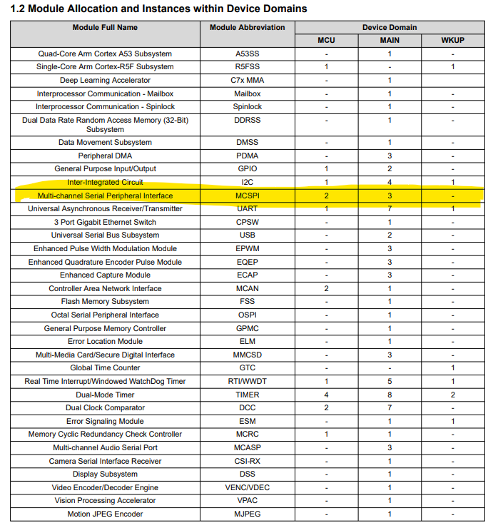
Q:Is my understanding correct that the AM62A's main domain (A53) can control the peripherals of the MCU domain (R5F)?
Specifically, is it correct to say that the main domain (A53) can control a total of 5 SPI interfaces, consisting of 3 main SPI and 2 MCU SPI?

My understand from the following URL that the MCU domain can control some peripherals of the main domain.
AM62Ax MCU+ SDK: Accessing main and wakeup domain peripherals from MCU domain
In MCU+SDK v11.1, I have confirmed that importing "mcspi_loopback_am62ax-sk_a53ss0-0_nortos_gcc-aarch64" and configuring it in SysConfig allows it to build.
Based on TRM section "3.3 Initiator/Target Connectivity," I understand they are internally connected.

image.png

Best regards,
O.H

  • Hello,

    Please allow me sometime to respond to our open queries.

    Thanks,

    Vaibhav

  • Hello,

    From A53, MCU_R5 & R5:

    SPI0/1/2 can be used in Interrupt/Polled/DMA modes.

    MCU_SPI0/1 can be used in Interrupt/Polled modes.

    I have seen the above observation from the SysConfig GUI tool for each of A53, MCU-R5 and R5 examples.

    A simple way to test this out would be to run MCSPI Loopback example, where you would just need to connect TX and RX pins, essentially the MCSPI D0 and D1 pins, via jumper cables.

    Hope this helps.

    Kind Regards,

    Vaibhav

  • Additionally please refer the MCSPI Integration Guide: e2e.ti.com/.../faq-sk-am64b-mcspi-integration-guide

  • Hello Vaibhav-san,

    Thank you for your supprots.

    I confirmed the following two projects on sk-AM62A-LP:

    • mcspi_loopback_am62ax-sk_c75ss0-0_freertos_ti-c7000
    • mcspi_loopback_am62ax-sk_mcu-r5fss0-0_nortos_ti-arm-clang

    As a result: The communication results differ as expected for both "C75" and "R5F" depending on whether D0 and D1 are short-circuited (for both spi0 and mcuspi0).

    • On .sycfg, the .out files were generated activating spi0 or mcu_spi0 from either project (a total of 4 patterns).
    • Then, from the .ccxml file, "start project-less debug" → connect to the target core → "load program" → if D0 and D1 are short-circuited, "all tests have passed!!"
    • Disconnect from the core once → power cycle → reload → if D0 and D1 are not short-circuited, "some tests have failed!!"
    • After completely removing the default spi settings from .syscfg and then adding new spi settings, it seems to work stably.

    I have an additional question:

    Q2: Could you explain the reason for dividing the interfaces into main and MCU in the datasheet and TRM, etc.? Is it just reflected in the defaults in SDK and other similar places?

    Best regards,
    O.H

  • Hi,

    I confirmed the following two projects on sk-AM62A-LP:

    • mcspi_loopback_am62ax-sk_c75ss0-0_freertos_ti-c7000
    • mcspi_loopback_am62ax-sk_mcu-r5fss0-0_nortos_ti-arm-clang

    As a result: The communication results differ as expected for both "C75" and "R5F" depending on whether D0 and D1 are short-circuited (for both spi0 and mcuspi0).

    • On .sycfg, the .out files were generated activating spi0 or mcu_spi0 from either project (a total of 4 patterns).
    • Then, from the .ccxml file, "start project-less debug" → connect to the target core → "load program" → if D0 and D1 are short-circuited, "all tests have passed!!"
    • Disconnect from the core once → power cycle → reload → if D0 and D1 are not short-circuited, "some tests have failed!!"
    • After completely removing the default spi settings from .syscfg and then adding new spi settings, it seems to work stably.

    The reason for seeing this behaviour is because of how the example works. It sends data from TX to RX or D0 to D1 based on the configuration and hence the name loopback. If D0 and D1 are not connected then this example will show failure, as you have seen. So I hope there is no doubt regarding this area.

    Q2: Could you explain the reason for dividing the interfaces into main and MCU in the datasheet and TRM, etc.? Is it just reflected in the defaults in SDK and other similar places?

    Coming to question number 2, I would like to answer this primarily based on two aspects although there could be more.

    Timing and Safety.

    It is prevalent that if you are running an application on the R5 core/Main Domain then accessing peripherals/interfaces which are based out of Main Domain will have much lower latency compare to accessing peripherals from MCU/Other Domain which not Main Domain. Hence the latency aspect comes into the picture.

    Now coming to safety critical applications, mostly these run on the MCU domain, and hence lets suppose some peripheral is configured in the MCU domain, you do not want this to go down.

    Moreover, other use cases exist, for example, when performing reset, main domain gets reset, while the safety domain should not, as it might contain critical applications running. Hence, the peripheral distribution can be decided as per the use case.

    Hope this answers the question upto some extent. If not please let me know.

    Looking forward to your response.

    Kind Regards,

    Vaibhav

  • Hi 

    Thank you for your kind reply. Just to confirm, we understand the following, is it correct?

    • It is possible to control the MCU (R5F) SPI (MCU_SPI) from MAIN (A53), but latency will increase. Similarly, it is possible to control the MAIN (A53) SPI from the MCU (R5F), but latency will also increase.
    • As stated in the datasheet, the hardware SPI is connected to MAIN and MCU respectively. Although latency will increase, it is still possible to control them from the other side (MAIN or MCU).

    Best regads,
    O.H

  • Hi,

    Sorry for rush you. Is there any comment?

    Thank you for your kind reply. Just to confirm, we understand the following, is it correct?

    • It is possible to control the MCU (R5F) SPI (MCU_SPI) from MAIN (A53), but latency will increase. Similarly, it is possible to control the MAIN (A53) SPI from the MCU (R5F), but latency will also increase.
    • As stated in the datasheet, the hardware SPI is connected to MAIN and MCU respectively. Although latency will increase, it is still possible to control them from the other side (MAIN or MCU).

    Best regards,
    O.H

  • Hello,

    Thanks for your patience, as I was out of office, the responses were delayed.

    • It is possible to control the MCU (R5F) SPI (MCU_SPI) from MAIN (A53), but latency will increase. Similarly, it is possible to control the MAIN (A53) SPI from the MCU (R5F), but latency will also increase.
    • As stated in the datasheet, the hardware SPI is connected to MAIN and MCU respectively. Although latency will increase, it is still possible to control them from the other side (MAIN or MCU).

    This is a correct understanding.

    Kind Regards,

    Vaibhav

  • Hello,

    Thank you for your supports. I understood.

    Best regards,
    O.H