TDA4VE-Q1: TDA4VE Power Down Sequence Issue

Part Number: TDA4VE-Q1


Dear TI Expert.

We use TDA4VE as our project solution.

The following is our power-down sequence diagram.


image.png

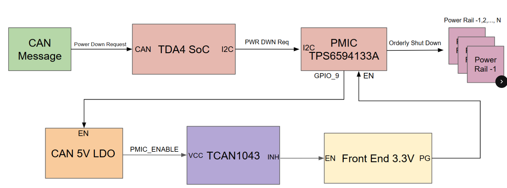
Our ECU has a sleep mode. When SoC execute the sleep command. SoC will shut down the PMIC vias IIC interface to make sure that the SoC Power-down sequence can meet the requirement.

When PMIC fully power down,then GPIO9 will turn low to disable CAN5V LDO.  If we disable CAN_5V output, then VCC for TCAN1043A will be zero, so TCAN1043A will be in sleep mode, INH = High Impedance, then Front End 3V3 EN pin is low and disable Sys 3V3 output. 

image.png


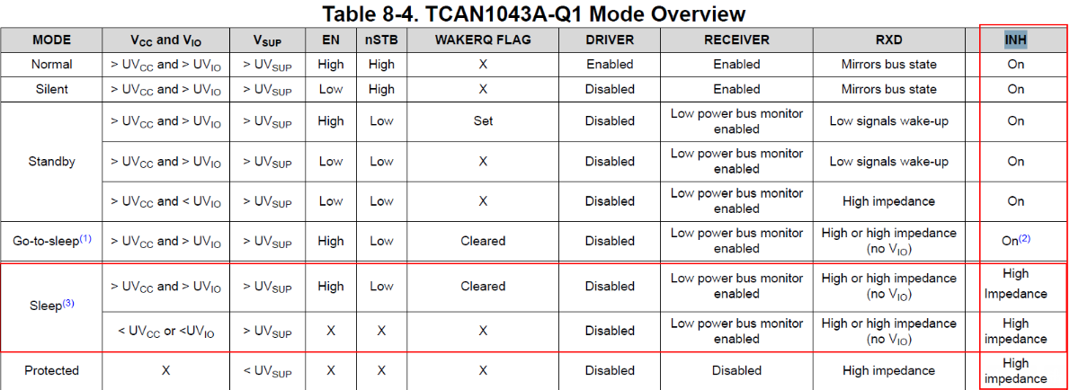
At this point, ECU finish the sleep opeation. When TCAN1043A receive a message from CAN BUS, INH pin will turn to High to reboot Front End 3V3 and then PMIC will reboot too. This is a dormant cycle.

However,there is such a situation that while SoC shut down PMIC vias IIC, if TCAN1043A receive messages from CAN BUS continuously. The PMIC will shut down as expected and INH pin will keep high all the time due to continuous messages from CAN BUS so that Front End 3V3 couldn't reboot.

If Front End 3V3 couldn't reboot, then PMIC can't reboot too. ECU will stuck in sleep mode without control.

Is there any recommendation that we can fix this issue? We can make sure to reboot Front End 3V3 if we want to execute sleep command.

Thanks!


  • If the CAN traffic is valid for keeping the SoC in active state, then perhaps you might consider the following options:

    1. If your product is not designed to use the SOC's GPIO or DDR Retention low power modes, then an independent system MCU or some discrete "glue logic" could be designed to cause PMIC's EN logic level to cycle low and high if the Front End 3.3V supply does not turn-off after a time-out period > normal Front End discharge time.

    2.If your product is designed to use the SOC's GPIO or DDR Retention low power modes, then consider transitioning to the SoC's GPIO Retention low power mode as step #1 towards a full system shut down before the Front End 3.3V 1st stage power is disabled. This would allow valid CAN traffic a means to reboot the SoC since the PDN-3x schemes supported by the TPS6594133A-Q1 PMIC provide an independent means to wake-up the SoC via the "SOC_PWR_WKn" net connection to PMIC's GPIO4, see snap-shot below of J784S4 EVM detailed PDN-3A block diagram and Note #4.  The entire J784S4 EVM detailed PDN-3A block diagram is available as part of the EVM design source zip file from TI website (J784S4XEVM Evaluation board | TI.com).

    Additional information on entering & exiting low power modes can be found in the TPS6594133A User's Guide (Powering Jacinto 7 SoC For Isolated Power Groups With TPS6594133A-Q1 + Dual HCPS (Rev. A)), as shown below.