This thread has been locked.

If you have a related question, please click the "Ask a related question" button in the top right corner. The newly created question will be automatically linked to this question.

AM62P: Causes of the decrease in DRVVBUS terminal output level

Part Number: AM62P
Other Parts Discussed in Thread: SN74LV1T08

Hi team,
Currently, we are evaluating the USB interface as part of the assessment of a custom board equipped with the AM62P.

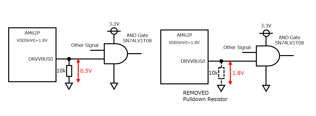
As shown in the following figure, the DRVVBUS of the AM62P on the custom board is connected to the input of the SN74LV1T08 (AND gate) via a 10k pull-down resistor. 
However, when DRVVBUS is outputting a high level, the expected voltage level is approximately 1.8V, but it only reaches about 0.5V.
On the other hand, removing the pull-down resistor results in the DRVVBUS output voltage being approximately 1.8V.

What could be the cause of the DRVVBUS output level dropping under these conditions?
Is the drive strength setting of the DRVVBUS terminal inappropriate? 

Thank you for your support.

image.png

  • Hello Tsubasa Hatada,

    This pin has by default enabled its pull-down resistor. External resistor to keep DRVVBUS during reset time is not needed. Please see snapshot from datasheet:

    Also, I don't know what is the Other Signal on the diagram, but please be aware that it can influence the USB controller's logic for Session Start and Session End. Keep this in mind in case you face issues with USB connection/enumeration.

    Thanks and Regards,

    Stan

  • Hello Stanislav Stilyanov,

    Thank you for your response.

    I overlooked the default pin configuration.
    Indeed, the internal pull-down is enabled by default.
    I understand that in 1.8V mode, the internal pull-down resistance is 15-30kΩ;however, I am concerned that the combined resistance value of the internal pull-down and the externally connected pull-down resistor does not seem to be low enough to prevent DRVVBUS from being driven.
    Could the specification reference for the internal pull-down resistor be incorrect?


    >Also, I don't know what is the Other Signal on the diagram, but please be aware that it can influence the USB controller's logic for Session Start and Session End.
    >Keep this in mind in case you face issues with USB connection/enumeration.

    I agree with that. The AND gate was added to control the load switch for VBUS exclusivity in order to support DRP USB-C.
    We have already confirmed that there is no impact on the USB controller's session start and end logic.

    Thank you for your support.

  • I am concerned that the combined resistance value of the internal pull-down and the externally connected pull-down resistor does not seem to be low enough to prevent DRVVBUS from being driven.

    You are right. 10k || 15k (min case) should not prevent active driving up to VDD under normal conditions.

    From your diagram I can only suspect this might be coming from 2 directions:

    • VDDSHV0 - there could be some additional, unwanted serial resistance on this power rail. Or, the power supply is overloaded (less probable) 
    • AND gate - For some reason, there is too low input resistance than normal that adds up. 

    Regards,

    Stan

  • Hi All, 

    Please isolate the ANDing logic and do a quick check.

    Regards,

    Sreenivasa