This thread has been locked.

If you have a related question, please click the "Ask a related question" button in the top right corner. The newly created question will be automatically linked to this question.

TDA4VEN-Q1: State of GPIO during system startup

Part Number: TDA4VEN-Q1

Hi.


On the evaluation board created with reference to the J722S EVM,
power supply interference occurred at startup.

For circuit debugging, when the signal line connected to GPIO1_8 (A26)
of the TDA4VEN was pulled up to VSYS_3V3, VDDSHV0, which is a separate
power supply, powered up in a sequence faster than usual.

Since GPIO1_8 is of the LVCMOS type, it is expected that a DC path is created
to VDDSHV0 through the IO’s P-MOS transistor.

Is the inference correct that GPIO1_8 will serve as a DC path to VDDSHV0
during system startup?
(What is the state of GPIO1_8 at system startup?)


VDDSHV0_BOOT_trouble.png

  • Hi Furuna,

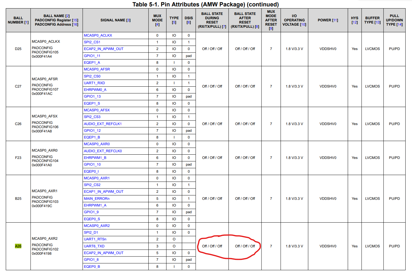
    Thank you for your inquiry. Table 5.1 in the datasheet shows the default pin behavior during reset and after reset is de-asserted. For A26, the pin should be floating. See the table below.

    Best Regards,

    Miles

  • Hi Miles,

    Thank you for your reply.

    Regarding A26, you mentioned that "the pin should be floating", but I understand that Table 5-1 describes the state of the IO during and after reset; is that incorrect?

    If a load is connected in the external circuit, is it correct to understand that the A26 pin will function as an H output even during reset?

    In the operational check we conducted, the A26 pin exhibited behavior as if the P-MOS transistor were ON.

    Regards,

  • Furuna,

    For pin A26 the TX Buffer is disabled during reset which would mean the P-MOS transistor should be off. This would lead to the bus being pulled high by the resistor that is connected to the VSYS_3V3 supply as the supply is ramped up. 

    Would you be able to also provide the MCU_PORz signal in your capture?

    Best Regards,

    Miles

  • Hi. Miles,

    During the reset period, is it correct to understand that the A26 pin is in a high-impedance state,

    while the VDDSHV0 power supply and the bus (pulled up to VSYS_3V3) are connected with a high DC resistance?

    I added the MCU_PORz signal.

    However, since MCU_PORz is a signal where the PMIC RSTOUT output is inputted to the SoC, we think it is not suitable for

    the purpose of monitoring the IO state on the SoC side.

  • Hi Furuna,

    Thank you for providing the MCU_PORz signal. It helps to clarify the reset state of the IO while the issue is occurring. 

    Yes, A26 is in a high-impedance state during reset, and it does look to me like while the issue is occurring the VDDSHV0 supply rail is being pulled up by the VSYS_3V3 supply with a high DC resistance. I am unsure of how this is occurring though. 

    While I look into this more, could you answer if this measurement is being made in simulation or on a physical board?

    Best Regards,

    Miles

  • Hi Miles, 

    We are measuring on a physical board.

    Please tell me the impedance on the pull-up side in the high-impedance state.

    Best Regards,

  • Hi Furuna,

    After digging into this a little bit, by bringing the VSYS_3V3 rail and the GPIO pin high before the GPIO supply (VDDSHV0) the steady state max voltage on the GPIO pin is violating the max voltage spec of the IO supply voltage (currently 0V) + 0.3V. This is causing the PMOS to be reverse biased and causing the IO supply to then follow the VSYS_3V3 supply. You can find the following spec in table 6.1 of the datasheet.

    Would you be able to pull the bus up with either VDDSHV0 itself, or a supply that comes up after VDDSHV0?

    Best Regards,

    Miles

  • Hi. Miles

    Thank you for the explanation. I understood.

    I will modify the circuit considering the power sequence.

    Best Regards,