This thread has been locked.

If you have a related question, please click the "Ask a related question" button in the top right corner. The newly created question will be automatically linked to this question.

AM62L: Issues with EMMC communication

Part Number: AM62L
Other Parts Discussed in Thread: AM68

Hello!

Currently we have an issue with the EMMC communication, as it fails with some very specific set of data.
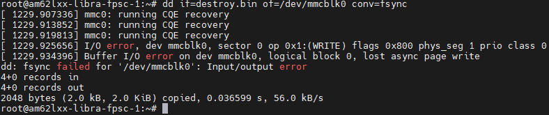
grafik.png

We did noticed the errata i2312, and tried to figure out what it actually means as the description is fairly generic. A test of all power supplies showed a pretty stable behaviour. We did also compare it to the EVK, which was slightly better, but not by much.
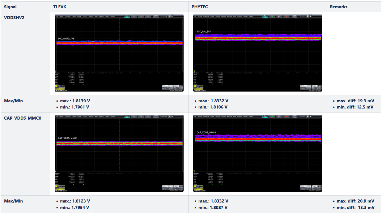
grafik.png

Do understand if your EVK would also generate errors, we did remove all capacitors on the bottom side, to basicly work against your errata, to see how much capacitors we would need. The result was the same, as the EVK did not generate these errors. 

As we are doing a redesign, our question would be, what we should do to not need a software fix for this problem? Which power supplies are effected for that errata? Which ripple are we allowed to have? Are there any recommendation for filter capacitors?

A schematic review by Ti was done, but I am happy to provide it again for you to take a look at it.

Cheers and thanks in advance.

  • Hi,

    Yes, can you please provide schematics from the PCB revision you are observing the errors? I've sent an e2e friend request.

    Thanks,

    Stan

  • Specifically the 1.8V IO supply noise is where problems can occur (VDDSHV2 on AM62L). Board measurements of the supply do not always show the true story of supply noise as this frequently can be filtered by measurement methods and the PDN itself. One possible way to get a sense of on die noise is to hold a single bit static high while toggling the rest, and check for fluctuations. 

    We do not have a spec for voltage ripple as this can be impacted by many system components, sustained burst size, and data pattern. 

    Are you able to implement a SW patch to test the workaround using single block writes and see if this resolves this issue? This may be one way to isolate supply as part of the issue. 

    Thanks,

    Chris 

  • Hi,

    The link below is the kernel patch of the sw workaround which Chris refers to. I just got accepted by the kernel upstream this morning. Please apply this patch to your kernel, it should recover the MMC I/O error.

    https://git.kernel.org/pub/scm/linux/kernel/git/ulfh/mmc.git/commit/?h=next&id=c7c6d4f5103864f73ee3a78bfd6da241f84197dd

  • Hi.

    Sorry, didn't get anything currently. But it seems that E2E is also a bit buggy at the moment. I get lots of errors, till I am able to log in.

  • If this is the same patch as in https://e2e.ti.com/support/processors-group/processors/f/processors-forum/1572388/am62l-processor-sdk-random-emmc-panics, than yes. This worked. But we would liked to change it also in hardware, so it behaves the same as in the EVK, even when it should have way worse AC coupeling as basicly every bypass capacitor was removed. So this is something that is puzzeling.

    But will forward the info of the patch beeing upstream  

     As repsonse to part of your post.

  • Do you mean just using them as GPIOs. Or rather using the eMMC in 1 Bit mode?

  • The new patch is functionally the same as the one you linked, with the difference of slightly structural change and handling of the non-CQE case. The new patch is the one which has been accepted by upstream kernel.

    I will defer to Chris and other hw folks on your hardware questions.

  • I'm not sure how much control you have over the data patter sent, but essentially if you can operate in 8b mode HS200 and send a bit pattern of 0xFF, 0x01, 0xFF, 0x01.. for example and measure data lane 0 it will give you an estimate. The source of noise is typically due to SSO so the fluctuation of data lane 0 in this example, which you would expect to remain at 1.8V, can help give a view of supply noise due to SSO. 

    Thanks,

    Chris 

  • Hi Bin, your patch being upstream is good news. Will you also send it to the mmc driver in u-boot upstream?

    Dominik

  • Hi Dominik,

    The U-Boot patch has not be created it yet. But it will be upstreamed, either by me or someone else in the development team.

  • Did you get the schematic? I did try to forward it to you via  

  • Hello phytecBSC,

    The hardware topic owner is currently unavailable.

    Please expect that a delay in his response might be possible.

    Thanks

    Best Regards

    Anastas Yordanov

  • Hello phytecBSC

    I am adding the inputs received from the expert:

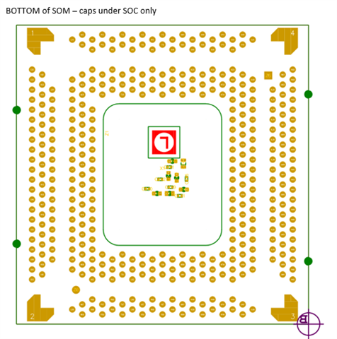
    Based on the pictures shared, it appears easier to put decap under the SOC but unable to put decap under the emmc

     We would want to  Emphasize the importance of decap for eMMC supply on SOC side. Recommend following the EVM.

    Based on the picture provided, the eMMC cannot have decaps underneath it due to board to board pins, and cannot have cap on the far right side.

    Perhaps optimizing the PDN to the eMMC is less critical than the PDN to the SOC supply pin.

     Regards,

    Sreenivasa

  • We are also not able to put one under the SoC, as we target a one sided PCB. The caps on the bottom have been put there to see if we would need them or not. 

    Well... we did remove every single cap on the EVM, there where none underneath the SoC (except for a apperently manditory decap for the uSD Interface). And there was still no error. So we created the worst case scenario, as the next best caps where in the range of about 2 cm (or so).

  • Hello phytecBSC

    Thank you.

    Well... we did remove every single cap on the EVM, there where none underneath the SoC (except for a apperently manditory decap for the uSD Interface). And there was still no error. So we created the worst case scenario, as the next best caps where in the range of about 2 cm (or so).

    I shared the inputs from the expert whi expressed concern on the PDN optimization.

    Can you please share the capacitor placement that you have in mind and i can get the experts thoughts.

    Regards,

    Sreenivasa

  • It is the same capacitor layout, just without any components on the bottom side.

  • Hello phytecBSC

    Thank you.

    Let me check with the expert.

    FYI, the expect is expected to be out of office until tuseday or wednesday.

    Please expect some delay in response.

    Regards,

    Sreenivasa

  • Any news on this?

  • Hello phytecBSC,

    Please expect that a certain delay is possible in the reply by the hardware expert (earliest tomorrow).

    Thanks

    Best Regards,

    Anastas Yordanov

  • Hello phytecBSC,

    Let me follow-up with the team and update you.

    Regards,

    Sreenivasa

  • Hello phytecBSC,

    It is the same capacitor layout, just without any components on the bottom side.

    Do you have the list of capacitors that was removed for each of the supply rail.

    Checking if you have removed any of the CAP_VDDSx capacitors.

    Regards,

    Sreenivasa

  • The capacitors have been attached to VDD_CORE, VDDA_1V8, VDD_DDR4 and VDDA_CORE (see send schematic for the actual SoC names). So no CAP domain. But I am not quite sure what this info would help, as we have the errors with and without them. And we see that even when we remove every CAP on your board it works... for whatever reason.

  • Hello phytecBSC,

    Thank you for letting us know.

    Let's the expert review and provide his feedback. Please expect that a certain delay is possible in the response.

    Thanks

    Best Regards,

    Anastas Yordanov

  • Hello phytecBSC,

    But I am not quite sure what this info would help,

    The reason for the question related to CAP_VDDSx is as below:

    For the IO bias generation to be stable a capacitor of 0.8-1/5uF is expected to be connected to the CAP_VDDSx pins. The capacitor is expected to be in the range considering tolerance, aging, temperature and DC bias.

    The IO bias generators that use the CAP_VDDSxxx pins for decoupling requires the capacitor connection to have < 2.5nH ESL and < 1 Ohm ESR for the entire connectivity loop and this includes external capacitor, package, and PCB contributions.  Achieving the resistance requirement may be possible, but it is already very difficult to achieve the inductance requirement when placing the capacitor on the bottom of the PCB under the BGA array.  The inductance requirement is likely to be impossible to achieve with no components on the bottom of the PCB.

     Regards,

    Sreenivasa

  • The inductance requirement is likely to be impossible to achieve with no components on the bottom of the PCB.

    Then how does it still work on your EVM, when I remove ALL caps (except for the one for the SD Interface) on the bottom of the PCB? I looked at your layout, and the next best capacitor is about 2 cm or so away. What would the argument here? As the traces are fairly thin, you wouldn't even use the argument of a certain capacity due to the planes.

    It is all nice and fine, and most likely absolutely correct, that you give me all the recommendation you have to create the best layout/circuit. But it won't explain this strange behaviour that regardless of how I butcher your EVK it just works without any software patch.

    So... what is the difference? Is the delivered SoC revisions faulty or to old? Are the ones used for the EVK special selected known good ones?

    But I waited for the last 2 months. So I can wait a little longer for an answer of your expert.

  • Hello, 

    I can understand the challenge here, but I don't know that we will have a good answer as to why the EVM wouldn't fail with capacitors removed. Again, for this topic the focus is on the eMMC IO supply, VDDSHV2. Since this is related to supply noise, this is a system level consideration and can be related to layout, trace lengths, the attached memory device, possible resonances, the data pattern being transmitted, etc. There is no special screening or device selection for devices selected for EVMs. 

    In the effort to understand and characterize this issue there was no target PDN that could be derived to totally prevent failures alone because of the complexity of the full system impacting supply noise. This is why the recommended SW workaround is spacing out the transactions. While improving PDN to limit noise helps mitigate failures and reduce occurrence, the SW workaround is the only certain way to totally eliminate them. This SW workaround will reduce the possible extreme supply swings and prevent the transmit failure form occurring.  

    The bottom line is our recommendation is to use the SW workaround as a 100% confident PDN will likely be very hard to achieve. I hope this helps clarify. 

    Thanks,

    Chris 

  • It helped that you mentioned that there was no special consideration for the PDN like you have for the AM68 or so, as we used your EVM as reference for the used components.

    Then I guess I leave it as it is, and use your workaround.

    Thanks everyone for your patience.