AM2434: AM2434 GPMC Memory Configuration

Part Number: AM2434
Other Parts Discussed in Thread: SYSCONFIG

Hello,

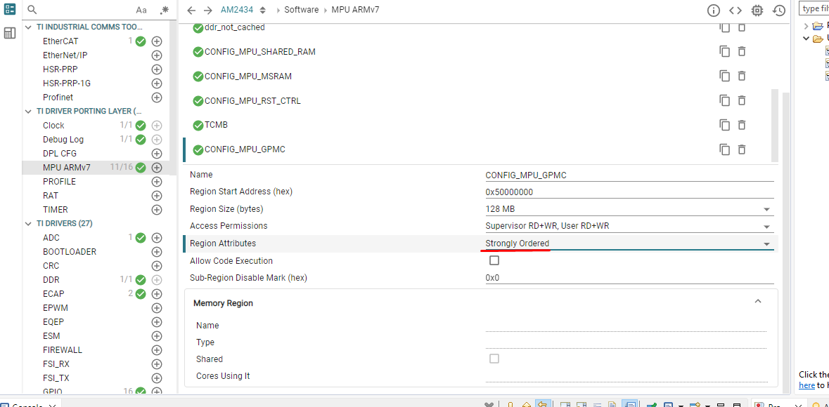
We are using a GPMC for communication to the FPGA. According to the example in the SDK we configured the memory as "Strongly ordered", We did some measurements and noticed that if we configure the memory as "Non cached" the time of writing/reading from GPMC is much faster.

Is it OK to switch to "Non cached" mode for FPGA communication? 

What are the consequences/penalties of switching to "Non cached" mode? 

image.png

thanks,

Sergei Pilipenko

  • Hello Sergei Pilipenko,

    I am Out of office today .

    I will provide reply  in one or two days .

    Regards,

    Anil

  • Hello,

    Any news?

    thanks,

    Sergei Pilipenko

  • Hello Sergei Pilipenko,

    Please look at my answers below .

    Strongly Ordered :

    - Every store reaches the bus in program order, with no reordering by the store buffer.
    - Every load is non-speculative — the CPU will not prefetch or predict reads to Strongly Ordered regions.
    - There is no write coalescing — each store is issued as a separate bus transaction.
    - Full ordering is maintained with respect to all other memory accesses before and after.

    These guarantees match exactly what an FPGA interface requires.


    Problems introduced by switching to Non-Cached Normal :

    If you change the MPU attribute to Non-Cached Normal, you lose the above guarantees:

    1. Write reordering by the store buffer
    The Cortex-R5F store buffer is allowed to reorder Normal memory writes relative to each other and relative to reads.

    Two consecutive FPGA register writes may arrive at the GPMC bus in a different order than your code
    issued them. For an FPGA protocol where register write sequence matters (e.g., address then data, command then trigger), this will cause incorrect FPGA behavior intermittently and is extremely difficult to debug.


    2. Speculative reads
    The CPU may issue speculative (prefetch) reads to Normal memory regions. A speculative read to an FPGA register that has a read side effect (FIFO pop, status clear, interrupt acknowledge) will corrupt your FPGA state even when your code never executed that read path. This is a silent data corruption with no indication of the cause.


    3. Read-after-write hazard
    Without the ordering guarantee, a read issued after a write may be executed before that write has reached the FPGA. Reading back a register to verify a write will return a stale value even though no cache is involved.


    On performance :

    The performance difference between Strongly Ordered and Non-Cached Normal on GPMC is not significant in practice. GPMC is a slow external bus (typical access latency tens of CPU cycles or more depending on wait states).
    The store buffer optimization that Non-Cached enables is relevant for fast internal memories. For GPMC-attached peripherals, the bus latency dominates and the ordering overhead of Strongly Ordered adds negligible additional cost.

    This is the correct and safe configuration for any memory-mapped I/O peripheral, including FPGA interfaces. The MCU+ SDK GPMC example (gpmc_flash_io) uses this configuration for this reason. So, we recommend to use with Strongly ordered .

    If you are seeing a specific performance concern with GPMC throughput, please share the measured throughput and access pattern — there may be GPMC timing parameter tuning (CS timing, ADV/OE/WE hold/setup counts) that can improve performance without compromising correctness.

    Regards,

    Anil.

  • Hi Anil,

    I did a little banchmark test:

    Non-Cached:

    Read 1000 X 16bit: Time taken for loop: 200617 cycles, average: 200 cycles
    Read 1000 X 32bit: Time taken for loop: 289599 cycles, average: 289 cycles
    Write 1000 X 16bit: Time taken for loop: 11217 cycles, average: 11 cycles
    Write 1000 X 32bit: Time taken for loop: 11611 cycles, average: 11 cycles

    Strngly-Ordered:

    Read 1000 X 16bit: Time taken for loop: 204627 cycles, average: 204 cycles
    Read 1000 X 32bit: Time taken for loop: 295306 cycles, average: 295 cycles
    Write 1000 X 16bit: Time taken for loop: 144266 cycles, average: 144 cycles
    Write 1000 X 32bit: Time taken for loop: 211408 cycles, average: 211 cycles

    as you can see strongly ordered is 10 times slower for Write commands.

    GPMC Configuration:

        // GPMC Configuration
        *(uint32_t *)0x3B000060 = 0x8001202;
        *(uint32_t *)0x3B000064 = 0xC0E00;
        *(uint32_t *)0x3B000068 = 0x30900;
        *(uint32_t *)0x3B00006C = 0xC036E19;
        *(uint32_t *)0x3B000070 = 0x10E0C0E;
        *(uint32_t *)0x3B000074 = 0x8F030000;

    ----------------------------

    Banchmark code:

    // Read 16 bit
    uint32_t start = CycleCounterP_getCount32();

    for (int i = 0; i < 1000; i++)
    {
    g_val += *(uint16_t*)0x50000000;
    }

    uint32_t end = CycleCounterP_getCount32();
    OSAL_PRINT_F("Read 1000 X 16bit: Time taken for loop: %u cycles, average: %u cycles" CRLF_MACRO, end - start, (end - start) / 1000);

    // Read 32bit
    start = CycleCounterP_getCount32();

    for (int i = 0; i < 1000; i++)
    {
    g_val += *(uint32_t*)0x50000000;
    }

    end = CycleCounterP_getCount32();
    OSAL_PRINT_F("Read 1000 X 32bit: Time taken for loop: %u cycles, average: %u cycles" CRLF_MACRO, end - start, (end - start) / 1000);

    // Write 16 bit
    start = CycleCounterP_getCount32();
    for (int i = 0; i < 1000; i++)
    {
    *(uint16_t*)0x50000000 = (uint16_t)g_val;
    }

    end = CycleCounterP_getCount32();
    OSAL_PRINT_F("Write 1000 X 16bit: Time taken for loop: %u cycles, average: %u cycles" CRLF_MACRO, end - start, (end - start) / 1000);

    // Write 32 bit
    start = CycleCounterP_getCount32();
    for (int i = 0; i < 1000; i++) {
    *(uint32_t*)0x50000000 = (uint32_t)g_val;
    }

    end = CycleCounterP_getCount32();
    OSAL_PRINT_F("Write 1000 X 32bit: Time taken for loop: %u cycles, average: %u cycles" CRLF_MACRO, end - start, (end - start) / 1000);

    ------------------------------------

    Sysconfig:

    /**
     * These arguments were used when this file was generated. They will be automatically applied on subsequent loads
     * via the GUI or CLI. Run CLI with '--help' for additional information on how to override these arguments.
     * @cliArgs --device "AM243x_ALV_beta" --part "ALV" --package "ALV" --context "r5fss0-0" --product "INDUSTRIAL_COMMUNICATIONS_SDK_AM243x@11.00.00"
     * @v2CliArgs --device "AM2434" --package "FCBGA (ALV)" --variant "AM2434-D" --context "r5fss0-0" --product "INDUSTRIAL_COMMUNICATIONS_SDK_AM243x@11.00.00"
     * @versions {"tool":"1.25.0+4268"}
     */
    
    /**
     * Import the modules used in this configuration.
     */
    const eeprom      = scripting.addModule("/board/eeprom/eeprom", {}, false);
    const eeprom1     = eeprom.addInstance();
    const flash       = scripting.addModule("/board/flash/flash", {}, false);
    const flash1      = flash.addInstance();
    const ram         = scripting.addModule("/board/ram/ram", {}, false);
    const ram1        = ram.addInstance();
    const ddr         = scripting.addModule("/drivers/ddr/ddr", {}, false);
    const ddr1        = ddr.addInstance();
    const ecap        = scripting.addModule("/drivers/ecap/ecap", {}, false);
    const ecap1       = ecap.addInstance();
    const ecap2       = ecap.addInstance();
    const gpio        = scripting.addModule("/drivers/gpio/gpio", {}, false);
    const gpio2       = gpio.addInstance();
    const gpio3       = gpio.addInstance();
    const gpio4       = gpio.addInstance();
    const gpio5       = gpio.addInstance();
    const i2c         = scripting.addModule("/drivers/i2c/i2c", {}, false);
    const i2c1        = i2c.addInstance();
    const mcspi       = scripting.addModule("/drivers/mcspi/mcspi", {}, false);
    const mcspi1      = mcspi.addInstance();
    const uart        = scripting.addModule("/drivers/uart/uart", {}, false);
    const uart1       = uart.addInstance();
    const udma        = scripting.addModule("/drivers/udma/udma", {}, false);
    const udma1       = udma.addInstance();
    const debug_log   = scripting.addModule("/kernel/dpl/debug_log");
    const mpu_armv7   = scripting.addModule("/kernel/dpl/mpu_armv7", {}, false);
    const mpu_armv71  = mpu_armv7.addInstance();
    const mpu_armv72  = mpu_armv7.addInstance();
    const mpu_armv73  = mpu_armv7.addInstance();
    const mpu_armv74  = mpu_armv7.addInstance();
    const mpu_armv75  = mpu_armv7.addInstance();
    const mpu_armv76  = mpu_armv7.addInstance();
    const mpu_armv77  = mpu_armv7.addInstance();
    const mpu_armv78  = mpu_armv7.addInstance();
    const mpu_armv79  = mpu_armv7.addInstance();
    const mpu_armv710 = mpu_armv7.addInstance();
    const mpu_armv711 = mpu_armv7.addInstance();
    const mpu_armv712 = mpu_armv7.addInstance();
    const mpu_armv713 = mpu_armv7.addInstance();
    const enet_cpsw   = scripting.addModule("/networking/enet_cpsw/enet_cpsw", {}, false);
    const enet_cpsw1  = enet_cpsw.addInstance();
    const tinyusb     = scripting.addModule("/usb/tinyusb/tinyusb", {}, false);
    const tinyusb1    = tinyusb.addInstance();
    
    /**
     * Write custom configuration values to the imported modules.
     */
    eeprom1.$name      = "CONFIG_EEPROM_POWER";
    eeprom1.i2cAddress = 0x52;
    
    flash1.$name                        = "CONFIG_FLASH0";
    flash1.device                       = "CUSTOM_FLASH";
    flash1.fname                        = "GD25B256E";
    flash1.flashSize                    = 33554432;
    flash1.flashManfId                  = "0xC8";
    flash1.flashDeviceId                = "0x4019";
    flash1.flashBlockSize               = 65536;
    flash1.cmdBlockErase3B              = "0xD8";
    flash1.cmdSectorErase3B             = "0x20";
    flash1.cmdExtType                   = "NONE";
    flash1.xspiWipRdCmd                 = "0x00";
    flash1.xspiWipReg                   = "0x00000000";
    flash1.idNumBytes                   = 5;
    flash1.dummyId8                     = 0;
    flash1.fourByteEnableSeq            = "0x01";
    flash1.flashDeviceBusyTimeout       = 72000000;
    flash1.flashPageProgTimeout         = 256;
    flash1.protocol                     = "1s_1s_4s";
    flash1.cmdRd                        = "0x6C";
    flash1.cmdWr                        = "0x34";
    flash1.dummyClksCmd                 = 0;
    flash1.dummyClksRd                  = 8;
    flash1.flashQeType                  = "6";
    flash1.proto_isAddrReg              = false;
    flash1.dummy_isAddrReg              = false;
    flash1.strDtr_isAddrReg             = false;
    flash1.peripheralDriver.$name       = "CONFIG_OSPI0";
    flash1.peripheralDriver.child.$name = "drivers_ospi_v0_ospi_v0_template0";
    
    ram1.$name                                        = "CONFIG_RAM0";
    ram1.parallelRamDriver.$name                      = "board_ram_parallelRam_parallelram0";
    ram1.parallelRamDriver.sleepEnGpioDriver.$name    = "CONFIG_GPIO1";
    ram1.parallelRamDriver.psramDriver.$name          = "CONFIG_GPMC0";
    ram1.parallelRamDriver.psramDriver.GPMC.A1.$used  = false;
    ram1.parallelRamDriver.psramDriver.GPMC.A2.$used  = false;
    ram1.parallelRamDriver.psramDriver.GPMC.A3.$used  = false;
    ram1.parallelRamDriver.psramDriver.GPMC.A4.$used  = false;
    ram1.parallelRamDriver.psramDriver.GPMC.A5.$used  = false;
    ram1.parallelRamDriver.psramDriver.GPMC.A6.$used  = false;
    ram1.parallelRamDriver.psramDriver.GPMC.A7.$used  = false;
    ram1.parallelRamDriver.psramDriver.GPMC.A8.$used  = false;
    ram1.parallelRamDriver.psramDriver.GPMC.A9.$used  = false;
    ram1.parallelRamDriver.psramDriver.GPMC.A10.$used = false;
    ram1.parallelRamDriver.psramDriver.GPMC.A11.$used = false;
    ram1.parallelRamDriver.psramDriver.GPMC.A12.$used = false;
    ram1.parallelRamDriver.psramDriver.GPMC.A13.$used = false;
    ram1.parallelRamDriver.psramDriver.GPMC.A14.$used = false;
    ram1.parallelRamDriver.psramDriver.GPMC.A15.$used = false;
    ram1.parallelRamDriver.psramDriver.GPMC.A16.$used = false;
    ram1.parallelRamDriver.psramDriver.GPMC.A17.$used = false;
    ram1.parallelRamDriver.psramDriver.GPMC.A18.$used = false;
    ram1.parallelRamDriver.psramDriver.GPMC.A19.$used = false;
    ram1.parallelRamDriver.psramDriver.GPMC.A20.$used = false;
    ram1.parallelRamDriver.psramDriver.GPMC.A21.$used = false;
    
    ddr1.$name                    = "CONFIG_DDR0";
    ddr1.ddrConfigIncludeFileName = "../../board_ddrReginit_GD_DBI_CL14_bitswap.h";
    
    ecap1.$name                    = "ECAP_AX1_IPM_TEMP";
    ecap1.ECAP.$assign             = "ECAP2";
    ecap1.ECAP.IN_APWM_OUT.$assign = "MCAN1_RX";
    
    ecap2.$name                    = "ECAP_AX2_IPM_TEMP";
    ecap2.ECAP.$assign             = "ECAP1";
    ecap2.ECAP.IN_APWM_OUT.$assign = "MCAN1_TX";
    
    gpio2.$name                    = "CONFIG_GPIO0";
    gpio2.pinDir                   = "OUTPUT";
    gpio2.useMcuDomainPeripherals  = true;
    gpio2.MCU_GPIO.$assign         = "MCU_GPIO0";
    gpio2.MCU_GPIO.gpioPin.$assign = "MCU_SPI1_CS0";
    
    gpio3.$name          = "GPIO_FPGA_nPROGRAM";
    gpio3.pinDir         = "OUTPUT";
    gpio3.GPIO_n.$assign = "I2C1_SDA";
    
    gpio4.$name          = "GPIO_FPGA_nINIT";
    gpio4.GPIO_n.$assign = "UART0_CTSn";
    
    gpio5.$name          = "GPIO_EEPROM_WP";
    gpio5.pinDir         = "OUTPUT";
    gpio5.GPIO_n.$assign = "I2C1_SCL";
    
    eeprom1.peripheralDriver = i2c1;
    i2c1.$name               = "CONFIG_I2C_EEPROM_AND_POWER_TEMP";
    i2c1.enableIntr          = false;
    i2c1.I2C.$assign         = "I2C0";
    i2c1.I2C.SCL.$assign     = "I2C0_SCL";
    i2c1.I2C.SDA.$assign     = "I2C0_SDA";
    i2c1.I2C_child.$name     = "drivers_i2c_v0_i2c_v0_template0";
    
    mcspi1.$name                   = "CONFIG_SPI_FPGA";
    mcspi1.inputSelect             = "0";
    mcspi1.dpe0                    = "DISABLE";
    mcspi1.dpe1                    = "ENABLE";
    mcspi1.intrEnable              = "POLLED";
    mcspi1.mcspiChannel[0].$name   = "CONFIG_MCSPI_CH0";
    mcspi1.mcspiChannel[0].bitRate = 25000000;
    mcspi1.child.$name             = "drivers_mcspi_v0_mcspi_v0_template0";
    
    uart1.intrEnable   = "DISABLE";
    uart1.$name        = "CONFIG_UART_CONSOLE";
    uart1.UART.$assign = "USART1";
    
    const uart_v0_template  = scripting.addModule("/drivers/uart/v0/uart_v0_template", {}, false);
    const uart_v0_template1 = uart_v0_template.addInstance({}, false);
    uart_v0_template1.$name = "drivers_uart_v0_uart_v0_template0";
    uart1.child             = uart_v0_template1;
    
    udma1.$name = "CONFIG_UDMA0";
    
    debug_log.enableLogZoneWarning = false;
    debug_log.enableLogZoneError   = false;
    debug_log.enableMemLog         = true;
    debug_log.enableSharedMemLog   = true;
    
    mpu_armv71.$name             = "CONFIG_MPU_REGION0";
    mpu_armv71.size              = 31;
    mpu_armv71.attributes        = "Device";
    mpu_armv71.accessPermissions = "Supervisor RD+WR, User RD";
    mpu_armv71.allowExecute      = false;
    
    mpu_armv72.size              = 15;
    mpu_armv72.accessPermissions = "Supervisor RD+WR, User RD";
    mpu_armv72.$name             = "TCMA";
    
    mpu_armv73.baseAddr          = 0x41010000;
    mpu_armv73.size              = 15;
    mpu_armv73.accessPermissions = "Supervisor RD+WR, User RD";
    mpu_armv73.$name             = "TCMB";
    
    mpu_armv74.baseAddr = 0x70000000;
    mpu_armv74.$name    = "MSRAM";
    mpu_armv74.size     = 21;
    
    mpu_armv75.$name    = "DDR";
    mpu_armv75.baseAddr = 0x98000000;
    mpu_armv75.size     = 27;
    
    mpu_armv76.$name             = "CONFIG_MPU_REGION5";
    mpu_armv76.accessPermissions = "Supervisor RD+WR, User RD";
    mpu_armv76.baseAddr          = 0xA5000000;
    mpu_armv76.size              = 23;
    mpu_armv76.attributes        = "NonCached";
    
    mpu_armv77.baseAddr          = 0x60000000;
    mpu_armv77.accessPermissions = "Supervisor RD+WR, User RD";
    mpu_armv77.attributes        = "Device";
    mpu_armv77.$name             = "FLASH";
    mpu_armv77.size              = 25;
    
    mpu_armv78.$name        = "CONFIG_MPU_REGION_SHARED_RAM";
    mpu_armv78.baseAddr     = 0x701DC000;
    mpu_armv78.allowExecute = false;
    mpu_armv78.attributes   = "NonCached";
    mpu_armv78.size         = 13;
    
    mpu_armv79.$name    = "CONFIG_MPU_REGION_MSRAM";
    mpu_armv79.baseAddr = 0x701DE000;
    mpu_armv79.size     = 13;
    
    mpu_armv710.$name        = "DDR_NO_CACHE";
    mpu_armv710.baseAddr     = 0x90100000;
    mpu_armv710.size         = 16;
    mpu_armv710.attributes   = "NonCached";
    mpu_armv710.allowExecute = false;
    
    mpu_armv711.$name        = "SRAM_NC";
    mpu_armv711.attributes   = "NonCached";
    mpu_armv711.size         = 15;
    mpu_armv711.allowExecute = false;
    mpu_armv711.baseAddr     = 0x701D0000;
    
    mpu_armv712.$name        = "DDR_SHARED_MEMORY";
    mpu_armv712.baseAddr     = 0x9FC00000;
    mpu_armv712.size         = 22;
    mpu_armv712.attributes   = "NonCached";
    mpu_armv712.allowExecute = false;
    
    mpu_armv713.$name        = "CONFIG_MPU_GPMC";
    mpu_armv713.baseAddr     = 0x50000000;
    mpu_armv713.size         = 27;
    mpu_armv713.allowExecute = false;
    mpu_armv713.attributes   = "Device";
    
    enet_cpsw1.$name                       = "CONFIG_ENET_CPSW0";
    enet_cpsw1.LargePoolPktCount           = 32;
    enet_cpsw1.PktInfoOnlyEnable           = true;
    enet_cpsw1.macOnlyEn_hostPort          = true;
    enet_cpsw1.macOnlyEn_macPort1          = true;
    enet_cpsw1.macOnlyEn_macPort2          = true;
    enet_cpsw1.mdioMode                    = "MDIO_MODE_MANUAL";
    enet_cpsw1.DisableMacPort2             = true;
    enet_cpsw1.customBoardEnable           = true;
    enet_cpsw1.MDIO.MDC.$assign            = "PRG1_MDIO0_MDC";
    enet_cpsw1.MDIO.MDIO.$assign           = "PRG1_MDIO0_MDIO";
    enet_cpsw1.txDmaChannel[0].$name       = "ENET_DMA_TX_CH0";
    enet_cpsw1.rxDmaChannel[0].$name       = "ENET_DMA_RX_CH0";
    enet_cpsw1.netifInstance.create(1);
    enet_cpsw1.netifInstance[0].$name      = "NETIF_INST_ID0";
    enet_cpsw1.RGMII.$assign               = "CPSW";
    enet_cpsw1.RGMII.RGMII1_RD0.$assign    = "PRG1_PRU1_GPO5";
    enet_cpsw1.RGMII.RGMII1_RD1.$assign    = "PRG1_PRU1_GPO8";
    enet_cpsw1.RGMII.RGMII1_RD2.$assign    = "PRG1_PRU1_GPO18";
    enet_cpsw1.RGMII.RGMII1_RD3.$assign    = "PRG1_PRU1_GPO19";
    enet_cpsw1.RGMII.RGMII1_RX_CTL.$assign = "PRG1_PRU0_GPO5";
    enet_cpsw1.RGMII.RGMII1_RXC.$assign    = "PRG1_PRU0_GPO8";
    enet_cpsw1.RGMII.RGMII1_TD0.$assign    = "PRG1_PRU1_GPO7";
    enet_cpsw1.RGMII.RGMII1_TD1.$assign    = "PRG1_PRU1_GPO9";
    enet_cpsw1.RGMII.RGMII1_TD2.$assign    = "PRG1_PRU1_GPO10";
    enet_cpsw1.RGMII.RGMII1_TD3.$assign    = "PRG1_PRU1_GPO17";
    enet_cpsw1.RGMII.RGMII1_TX_CTL.$assign = "PRG1_PRU0_GPO9";
    enet_cpsw1.RGMII.RGMII1_TXC.$assign    = "PRG1_PRU0_GPO10";
    
    const udma2        = udma.addInstance({}, false);
    enet_cpsw1.udmaDrv = udma2;
    mcspi1.udmaDriver  = udma2;
    
    tinyusb1.$name = "CONFIG_TINYUSB0";
    
    /**
     * Pinmux solution for unlocked pins/peripherals. This ensures that minor changes to the automatic solver in a future
     * version of the tool will not impact the pinmux you originally saw.  These lines can be completely deleted in order to
     * re-solve from scratch.
     */
    flash1.peripheralDriver.OSPI.$suggestSolution                     = "OSPI0";
    flash1.peripheralDriver.OSPI.CLK.$suggestSolution                 = "OSPI0_CLK";
    flash1.peripheralDriver.OSPI.CSn0.$suggestSolution                = "OSPI0_CSn0";
    flash1.peripheralDriver.OSPI.DQS.$suggestSolution                 = "OSPI0_DQS";
    flash1.peripheralDriver.OSPI.D7.$suggestSolution                  = "OSPI0_D7";
    flash1.peripheralDriver.OSPI.D6.$suggestSolution                  = "OSPI0_D6";
    flash1.peripheralDriver.OSPI.D5.$suggestSolution                  = "OSPI0_D5";
    flash1.peripheralDriver.OSPI.D4.$suggestSolution                  = "OSPI0_D4";
    flash1.peripheralDriver.OSPI.D3.$suggestSolution                  = "OSPI0_D3";
    flash1.peripheralDriver.OSPI.D2.$suggestSolution                  = "OSPI0_D2";
    flash1.peripheralDriver.OSPI.D1.$suggestSolution                  = "OSPI0_D1";
    flash1.peripheralDriver.OSPI.D0.$suggestSolution                  = "OSPI0_D0";
    ram1.parallelRamDriver.sleepEnGpioDriver.GPIO_n.$suggestSolution  = "OSPI0_LBCLKO";
    ram1.parallelRamDriver.psramDriver.GPMC.$suggestSolution          = "GPMC0";
    ram1.parallelRamDriver.psramDriver.GPMC.OEn_REn.$suggestSolution  = "GPMC0_OEn_REn";
    ram1.parallelRamDriver.psramDriver.GPMC.ADVn_ALE.$suggestSolution = "GPMC0_ADVn_ALE";
    ram1.parallelRamDriver.psramDriver.GPMC.WEn.$suggestSolution      = "GPMC0_WEn";
    ram1.parallelRamDriver.psramDriver.GPMC.CSn0.$suggestSolution     = "GPMC0_CSn0";
    ram1.parallelRamDriver.psramDriver.GPMC.BE1n.$suggestSolution     = "GPMC0_BE1n";
    ram1.parallelRamDriver.psramDriver.GPMC.BE0n_CLE.$suggestSolution = "GPMC0_BE0n_CLE";
    ram1.parallelRamDriver.psramDriver.GPMC.AD0.$suggestSolution      = "GPMC0_AD0";
    ram1.parallelRamDriver.psramDriver.GPMC.AD1.$suggestSolution      = "GPMC0_AD1";
    ram1.parallelRamDriver.psramDriver.GPMC.AD2.$suggestSolution      = "GPMC0_AD2";
    ram1.parallelRamDriver.psramDriver.GPMC.AD3.$suggestSolution      = "GPMC0_AD3";
    ram1.parallelRamDriver.psramDriver.GPMC.AD4.$suggestSolution      = "GPMC0_AD4";
    ram1.parallelRamDriver.psramDriver.GPMC.AD5.$suggestSolution      = "GPMC0_AD5";
    ram1.parallelRamDriver.psramDriver.GPMC.AD6.$suggestSolution      = "GPMC0_AD6";
    ram1.parallelRamDriver.psramDriver.GPMC.AD7.$suggestSolution      = "GPMC0_AD7";
    ram1.parallelRamDriver.psramDriver.GPMC.AD8.$suggestSolution      = "GPMC0_AD8";
    ram1.parallelRamDriver.psramDriver.GPMC.AD9.$suggestSolution      = "GPMC0_AD9";
    ram1.parallelRamDriver.psramDriver.GPMC.AD10.$suggestSolution     = "GPMC0_AD10";
    ram1.parallelRamDriver.psramDriver.GPMC.AD11.$suggestSolution     = "GPMC0_AD11";
    ram1.parallelRamDriver.psramDriver.GPMC.AD12.$suggestSolution     = "GPMC0_AD12";
    ram1.parallelRamDriver.psramDriver.GPMC.AD13.$suggestSolution     = "GPMC0_AD13";
    ram1.parallelRamDriver.psramDriver.GPMC.AD14.$suggestSolution     = "GPMC0_AD14";
    ram1.parallelRamDriver.psramDriver.GPMC.AD15.$suggestSolution     = "GPMC0_AD15";
    ram1.parallelRamDriver.psramDriver.GPMC.WAIT0.$suggestSolution    = "GPMC0_WAIT0";
    mcspi1.SPI.$suggestSolution                                       = "SPI0";
    mcspi1.SPI.CLK.$suggestSolution                                   = "SPI0_CLK";
    mcspi1.SPI.D0.$suggestSolution                                    = "SPI0_D0";
    mcspi1.SPI.D1.$suggestSolution                                    = "SPI0_D1";
    mcspi1.mcspiChannel[0].CSn.$suggestSolution                       = "SPI0_CS0";
    uart1.UART.RXD.$suggestSolution                                   = "UART1_RXD";
    uart1.UART.TXD.$suggestSolution                                   = "UART1_TXD";
    enet_cpsw1.MDIO.$suggestSolution                                  = "MDIO0";
    tinyusb1.USB.$suggestSolution                                     = "USB0";
    tinyusb1.USB.DRVVBUS.$suggestSolution                             = "USB0_DRVVBUS";
    

    Thanks,

    Sergei

  • Hello Sergei,

    My suggestion is that instead of using non-cached memory, try using cached MPU settings for the GPMC Memory and see the results.

    I hope the read performance will also improve.

    Please let me know the results

    Regards,

    Anil.

  • Hello Anil,

    With cached  memory, I have a few concerns around cache coherency and data consistency when accessing the memory from both sides. In particular, I want to make sure there are no issues with stale reads or delayed visibility of writes.

    How can we ensure data coherency in this setup?

    Could you please clarify if this approach has been tested in similar use cases, and whether there are any known limitations?

    Best regards,
    Sergei

  • Hello Sergei,

    Keeping the memory in non-cached mode means the CPU always reads data directly from memory instead of from cache.

    This requires more cycles and results in degraded performance compared to cached access.

    However, keeping the memory as cached is definitely not a problem with cache coherency because you are controlling GPMC in a single core only, not in other cores. This way, the data remains properly visible.

    When we configure the memory as cached with write-through policy, every cached write propagates immediately to memory:
    - All writes propagate immediately to NOR memory
    - Reads benefit from L1 D-cache acceleration
    - Single-core L1 cache management is straightforward
    - Data consistency is guaranteed

    Almost all memories are configured as cached to achieve better performance.

    I don't think there is any issue with the cached configuration.

    Regards,

    Anil.