This thread has been locked.

If you have a related question, please click the "Ask a related question" button in the top right corner. The newly created question will be automatically linked to this question.

AM6442: Optimizing AM64x PRU-ICSSG for Deterministic 40 MSPS Data Acquisition

Part Number: AM6442
Other Parts Discussed in Thread: ADC12DL040

Dear TI Support Team,

I am writing to inquire about the high-speed data acquisition capabilities of the AM64x Sitara processor, specifically using the PRU-ICSSG (Industrial Communication Subsystem) for a fast sampling application.

I am planning to interface an external ADC (specifically the ADC12DL040)or anyother to the AM64x Starter Kit. I have the following technical questions:

1. Sampling Rate: Can the PRU effectively handle a sampling rate of 40 MSPS for a 12-bit data stream?
2. Interface: Given the 40 MSPS requirement, which interface is recommended? I am currently looking at a Parallel CMOS interface using the PRU Expansion Header (J15). Is this the most efficient way to achieve single-cycle data capture?
3. Pin Mapping: Which specific pins on the  header are optimized for this type of parallel data acquisition to ensure minimal latency and deterministic behavior?
4. Resource Recommendations: Are there any existing PRU firmware examples or application notes for high-speed parallel ADC interfacing on the AM64x?

I appreciate your guidance on the best practices for this implementation

  • Hi Vijay sharma,

    1. Sampling Rate: Can the PRU effectively handle a sampling rate of 40 MSPS for a 12-bit data stream?

    SK-AM64B: Programmable Real-Time Unit Frequency - Processors - INTERNAL forum - Processors - INTERNAL - TI E2E support forums

    yes, please check above E2E

    Interface: Given the 40 MSPS requirement, which interface is recommended? I am currently looking at a Parallel CMOS interface using the PRU Expansion Header (J15). Is this the most efficient way to achieve single-cycle data capture?

    Yes, sampling using PRU is efficient way and save's cost replacing FPGA

    3. Pin Mapping: Which specific pins on the  header are optimized for this type of parallel data acquisition to ensure minimal latency and deterministic behavior?
    4. Resource Recommendations: Are there any existing PRU firmware examples or application notes for high-speed parallel ADC interfacing on the AM64x?

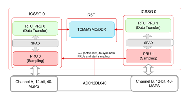
    I see PRU connector at J10 on AM64x starter kit, and all the PRU_GPI pins are available so map ADC_DATA_CHA [0:11] to PRU0_GPI [0:11] and 

    ADC_DATA_CHB [0:11] to PRU1_GPI [0:11] 


    we suggest 4 core solution as DCLK rate is at high rate in your case (please see attached image)


    sample PRU code: - 

    read_block:
    	wbs r31, 16
    	xout 15, &r2, 32 ; transfer last samples to ipc spad;
    	mov r2.w0, r31.w0
    
    	wbs r31, 16
    	mov r2.w2, r31.w0
    	set r2.w0,r2.w0, 15 ; set highest bit in r2 as status bit for xin on rtu
    
    	wbs r31, 16
    	mov r3.w0, r31.w0
    	nop
    
    	wbs r31, 16
    	mov r3.w2, r31.w0
    	nop
    
    	wbs r31, 16
    	mov r4.w0, r31.w0
    	nop
    
    	wbs r31, 16
    	mov r4.w2, r31.w0
    	nop
    
    	wbs r31, 16
    	mov r5.w0, r31.w0
    	nop
    
    	wbs r31, 16
    	mov r5.w2, r31.w0
    	nop
    
    	wbs r31, 16
    	mov r6.w0, r31.w0
    	nop
    
    	wbs r31, 16
    	mov r6.w2, r31.w0
    	nop
    
    	wbs r31, 16
    	mov r7.w0, r31.w0
    	nop
    
    	wbs r31, 16
    	mov r7.w2, r31.w0
    	nop
    
    	wbs r31, 16
    	mov r8.w0, r31.w0
    	nop
    
    	wbs r31, 16
    	mov r8.w2, r31.w0
    	nop
    
    	wbs r31, 16
    	mov r9.w0, r31.w0
    	nop
    
    	wbs r31, 16
    	mov r9.w2, r31.w0
    	qba read_block


    sample RTU code:- 

    main:
    	zero	&r0, 120
    	ldi R13, 0
    	ldi32 R14, 0x78000000 ; TCM address
    
    read_block: ; we have 3*16 = 48 cycles available at 100 Msps
    	xin 15, &r2, 32
    	qbbc read_block, r2.w0, 15
    	clr r2.w0, r2.w0, 15 ; clear status bit
    	xout 15, &r2.w0, 2 ; clear status bit
    	sbbo &r2, R14, R13, 32
    	add R13, R13, 32 ; we have written 16 samples, 2 byte each
    	; you can use ping-pong buffer to send the data to host (Refer PRU_IPC driver, uses TCM of R5F)
    	; documenation is at https://software-dl.ti.com/mcu-plus-sdk/esd/AM243X/11_02_00_24/exports/docs/api_guide_am243x/DRIVERS_PRU_IPC.html
    	; PRU_IPC macro's are available at "{mcu_plus_sdk_path}\source\pru_io\firmware\common" 
    	; PRU_IPC driver code is at "{mcu_plus_sdk_path}\source\pru_io\driver"
    	qba read_block


    unfortunately, we don't have any example / reference design in SDK with the requirements you mentioned.

    Use above sample code to get started and l
    et us know if you need any help in implementation.

    Thanks & regards,
    Manoj.

  • Dear Manoj,

    Thank you very much for the precise and detailed answers to my questions regarding the AM64x PRU-ICSSG data acquisition. I truly appreciate the technical guidance and the sample code provided for both the PRU and RTU cores.

    However, I noticed that the link provided in your response regarding the Programmable Real-Time Unit Frequency appears to be broken or leading to an internal page that I cannot access (as shown in the screenshot).

    Could you please provide the updated or correct source link for that information? Additionally, if there are any further documents or specific sections of the MCU+ SDK Documentation you recommend for this 40 MSPS implementation, please let me know.

    Thank you again for your support.

    Best regards,

    Vijay Sharma

  • Hi Vijay sharma,

    However, I noticed that the link provided in your response regarding the Programmable Real-Time Unit Frequency appears to be broken or leading to an internal page that I cannot access (as shown in the screenshot).

    okay, 

    1. Sampling Rate: Can the PRU effectively handle a sampling rate of 40 MSPS for a 12-bit data stream?

    yes,

    In short we can do parallel capture mode (16 bit) data uclock provides 166 MHz * 16 bit *2 (DDR) = 333 Msps or 5.3 Gbit bandwidth.

    using PRU0 to do rising edge capture and PRU1 falling edge capture of 16 bit.

    A sequence of 
    wbs r31, 16
    mov r2.w0, r31.w0

    at 333 MHz PRU

    This reaches the SoC data movement limits so, recommendation is to go max 100 Msps. 

    Below links along with sample code snippets shared previously will be helpful in creating the example: -  

    PRU assembly instructions:- https://github.com/TexasInstruments/open-pru/blob/main/docs/PRU%20Assembly%20Instruction%20Cheat%20Sheet.md

    GPIO toggle example :- 
    https://github.com/TexasInstruments/open-pru/tree/main/academy/gpio/gpio_toggle

    PRU ADC examples: -  AM64x MCU+ SDK: ADC

    Thanks & regards,
    Manoj