This thread has been locked.

If you have a related question, please click the "Ask a related question" button in the top right corner. The newly created question will be automatically linked to this question.

[FAQ] AM2434: Understanding UART Uniflash and OSPI Flash Programming

Part Number: AM2434
Other Parts Discussed in Thread: UNIFLASH, SYSCONFIG

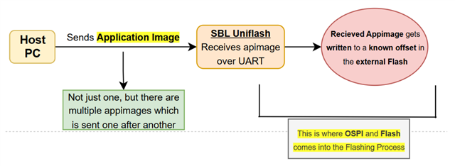
uart_uniflash.py allows to flash binaries to the flash on a EVM. UART is used as the transport or interface to send the file to flash to the EVM. When the uart_uniflash.py script is executed, a multi-stage process is initiated to program the external flash memory over UART. The below process occurs from the FLASH and OSPI perspective.


  • 1. Initial UART Bootloader Transfer

    After executing the below command on the PC,

      python uart_uniflash.py -p COM3 --cfg=sbl_prebuilt/am243x-evm/sbl_uart_uniflash.cfg

    The following takes place:

    • The script establishes a serial connection to the target device.
    • The ROM bootloader of the target device is waiting in UART boot mode which is configured via boot pins.
    • The script then sends the SBL UART Uniflash bootloader to the device over UART using the XMODEM protocol.
    • This SBL is then loaded into the internal RAM which is the OCMC RAM or MSRAM. There is no flash involvement till now.


    2. OSPI Controller Initialization done by the SBL

    Once SBL_UART_UNIFLASH is running on the target:

    • The OSPI Peripheral is configured with the following:
      • Clock configuration
      • Pin muxing for OSPI signals which would be the CLK, D0-D7, CS lines.
      • Protocol mode selection - Single, Quad, Octal.
    • Flash Device is detected:
      • SBL reads JEDEC ID by issuing a command 0x9Fh to identify flash manufacturer and the flash device.
      • It also configures the flash-specific parameters (sector size, page size, addressing mode) by reading the parameters present in the SFDP table.
      • It then initializes the flash device structure with proper command sequences.
  • 3. Flash Memory Preparation

    The below two process is usually carried out:

    • Flash Reset Sequence which resets the Flash device:
      •           OSPI_writeCmd(0x66);  // Reset Enable
        
                  OSPI_writeCmd(0x99);  // Reset Memory

        •  QE Bit Configuration (see QE Bit FAQ):
          • The SBL reads the current Status Register value for the QE Bit, and sets the Quad Enable bit if using Quad mode.
          • Then, the SBL writes back the modified Status Register.


        4. Flash Programming Operations

        For each file in the .cfg:

          --file=../path/to/app.release.appimage --operation=flash --flash-offset=0x80000


        The following happens:

        • a. Sector Erase:
          • Write Enable command and the Sector/Block Erase command is issued for the target offset.
          • Status Register is then polled, until the Write-In-Progress (WIP) bit clears.
        • b. Page Programming:
          • The data is transferred from PC to device over UART.
          • Write Enable command and the Page Program command is then issued.
          • The data is then written to the Flash.
          • Status Register is polled, until the WIP bit clears.


        5. Flash Controller State

        During programming, OSPI controller operates in:

        • SPI mode.
        • QSPI mode, if the QE bit is set.
        • DAC mode disabled: Direct Access Controller is not used during Flash wrties for Infineon Flash parts.
      • Role of FLASH After Flashing

        Once the flash is programmed and the device resets, the following happens:

        Boot Flow Overview

        Power-On → ROM Boot → Flash Detection → Load SBL → SBL Execution → Load Application

        1. ROM Bootloader Initialization

        • Boot Mode Selection: ROM reads boot pins to determine boot device, which is OSPI Bootmode in this case.
        • ROM then initializes OSPI controller in the basic SPI mode

        2. Flash Device Detection by ROM

        • ROM performs minimal flash initialization.
        • Important: ROM does NOT configure QE bit or advanced modes.


        3. Bootloader Image Header Read

        ROM reads from fixed offset in flash (typically 0x0), the Boot Image Header which contains the Magic Number, Image Size, Load Address, Entry Point.


      • 4. SBL Loading

        • ROM reads SBL binary from flash into internal RAM.
        • It uses basic SPI read commands and copies it to the load address specified in header.
        • It then transfers control to the SBL entry point.


        5. SBL now controls the Flash

        The SBL re-initializes OSPI for optimal performance by configuring the following:

        • Clock frequency: Increases OSPI clock to max supported, 166 MHz, or to the value specified in SysConfig of SBL.
        • Protocol: Configures QSPI or Octal mode.
        • DAC Mode: Can enable Direct Access Controller.
        • PHY Mode: Can Enable PHY for high-speed operation.
        • QE Bit: It can also verify and set the QE bit for Quad mode operations.


        6. Application Loading from Flash

        SBL reads application images from flash from the offset specified in the --flash-offset argument:

        Now, Each application can be:

        • Copied to RAM: SBL loads to MSRAM/DDR and CPU executes from RAM.
        • XIP (Execute-In-Place): CPU executes directly from flash, which requires DAC mode.