Part Number: DRA821U
Other Parts Discussed in Thread: SYSCONFIG, DRA821
Hi Team,
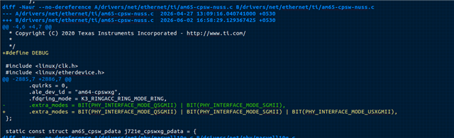
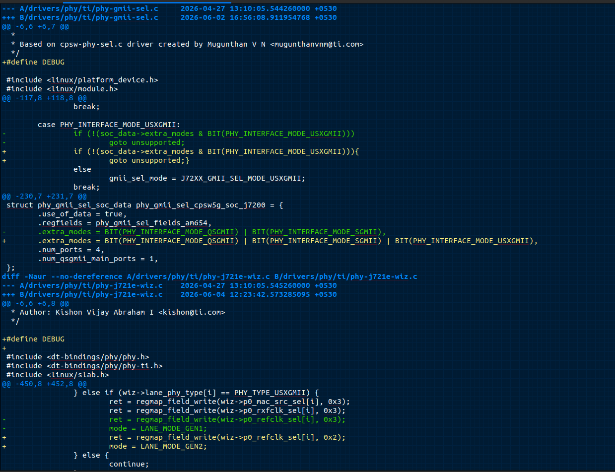
We are currently working on validating the 10G interface on the DRA821U processor. We had previously raised a support query (link below) and followed the same configuration in our setup. However, the Ethernet interface is not functioning as expected—link up and link down messages are being printed continuously.
Additionally, there have been updates to the TX and RX pin connections on our board. When we attempt to configure these TX/RX pins using the SysConfig tool, no corresponding entries are generated in the DTSI output. Now, we have only included the MDIO, MDC, and reset pins in the DTSI.
Could you please guide us with the following?
- Proper configuration of the 10G TX/RX pins in the DTSI
- Guidance to correctly bring up and validate the 10G interface
For reference, our previous query is included below:
https://e2e.ti.com/support/processors-group/processors/f/processors-forum/1608293/dra821u-guidance-required-for-implementing-10g-interface-on-dra821u/6203863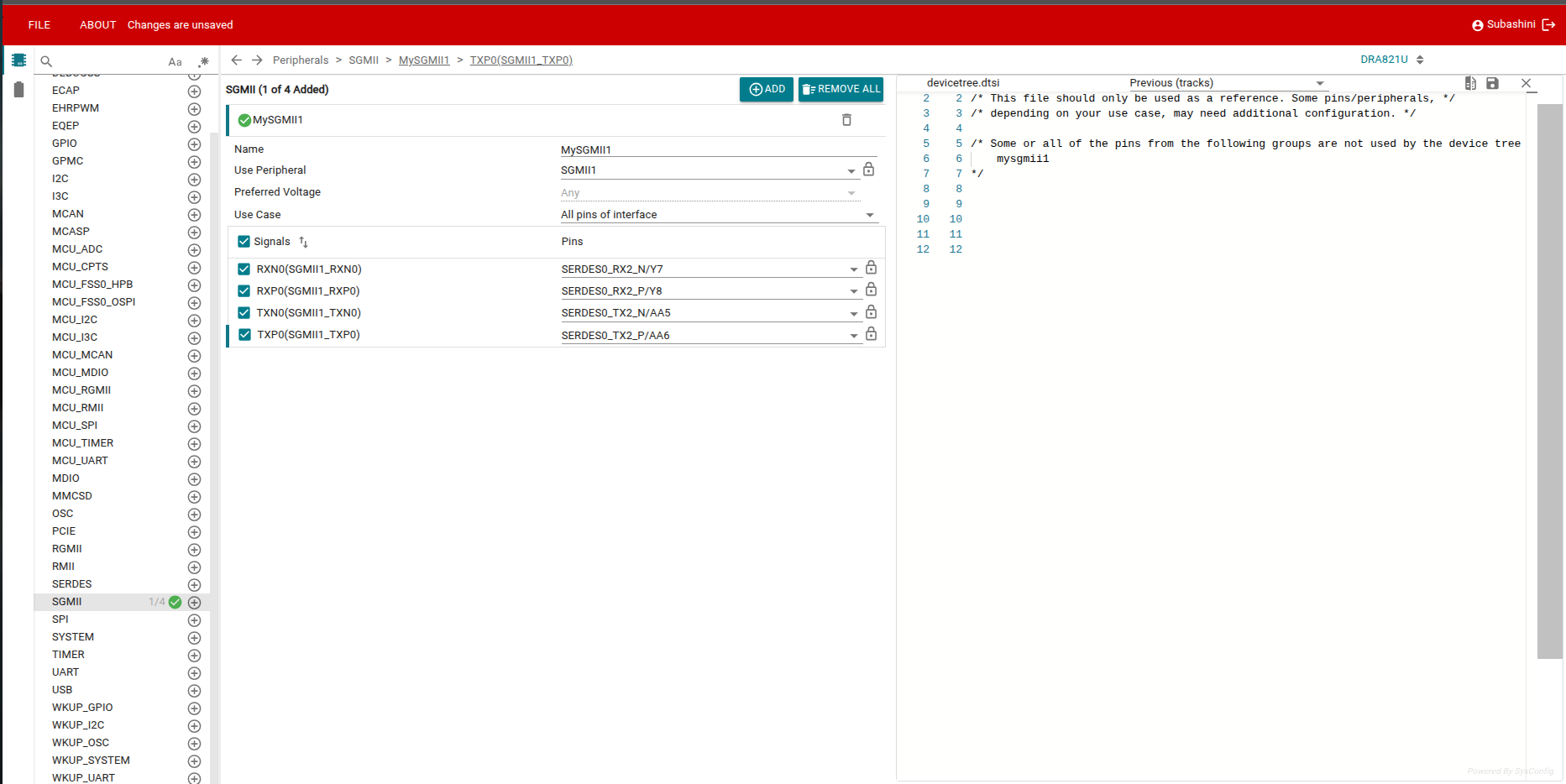
Pinmux
-------------
| Functionality | Pad name | Pin | Power group | GPIO no | INPUT/OUTPUT | IO LEVEL |
| SGMII1_TX0_N | MCU_RGMII1_TD1/MCU_RMII1_TXD1/WKUP_GPIO0_46 | B11 | VDDSHV2_MCU | - | Output | 1.8V, LVDS |
| SGMII1_TX0_P | MCU_RGMII1_TD0/MCU_RMII1_TXD0/WKUP_GPIO0_47 | D10 | VDDSHV2_MCU | - | Output | 1.8V, LVDS |
| SGMII1_RX0_N | MCU_RGMII1_RD1/MCU_RMII1_RXD1/WKUP_GPIO0_52 | B9 | VDDSHV2_MCU | - | Input | 1.8V, LVDS |
| SGMII1_RX0_P | MCU_RGMII1_RD0/MCU_RMII1_RXD0/WKUP_GPIO0_53 | A9 | VDDSHV2_MCU | - | Input | 1.8V, LVDS |
| ETH_10G_MDC | MCU_MDIO0_MDC/WKUP_GPIO0_55 | D9 | VDDSHV2_MCU | - | Output | 1.8V, LVCMOS |
| ETH_10G_MDIO | MCU_MDIO0_MDIO/WKUP_GPIO0_54 | C9 | VDDSHV2_MCU | - | Input/Output | 1.8V, LVCMOS |
| ETH_10G_RSTn(GPIO_A_1) | EXT_REFCLK1/SYNC1_OUT/CPTS0_HW2TSPUSH/UART3_TXD/SPI7_CLK/I2C1_SDA/GPIO0_59 | T3 | VDDSHV0 | GPIO0_59 | Output | 1.8V, LVCMOS |
| ETH_10G_INTn(GPIO_A_0) | ECAP0_IN_APWM_OUT/SYNC0_OUT/CPTS0_RFT_CLK/CPTS0_HW1TSPUSH/UART3_RXD/SPI7_CS0/I2C1_SCL/GPIO0_58 | U3 | VDDSHV0 | GPIO0_58 | Input | 1.8V, LVCMOS |
| RSTOUT(GPIO_A_2) | I2C0_SCL/GPIO0_56 | V3 | VDDSHV0 | GPIO0_56 | Output | 1.8V, LVCMOS |
| SGMII1_TX0_N | MCU_RGMII1_TD1/MCU_RMII1_TXD1/WKUP_GPIO0_46 | B11 | VDDSHV2_MCU | - | Output | 1.8V, LVDS |
| SGMII1_TX0_P | MCU_RGMII1_TD0/MCU_RMII1_TXD0/WKUP_GPIO0_47 | D10 | VDDSHV2_MCU | - | Output | 1.8V, LVDS |
| SGMII1_RX0_N | MCU_RGMII1_RD1/MCU_RMII1_RXD1/WKUP_GPIO0_52 | B9 | VDDSHV2_MCU | - | Input | 1.8V, LVDS |
| SGMII1_RX0_P | MCU_RGMII1_RD0/MCU_RMII1_RXD0/WKUP_GPIO0_53 | A9 | VDDSHV2_MCU | - | Input | 1.8V, LVDS |
Thanks and Regards,
Subashini