This thread has been locked.

If you have a related question, please click the "Ask a related question" button in the top right corner. The newly created question will be automatically linked to this question.

AM623: eMMC high speed mode timing

Part Number: AM623

On TRM, MMC_CTLCFG_HOST_CONTROL1 register field description: High speed mode otuputs data on clock rising edge. 
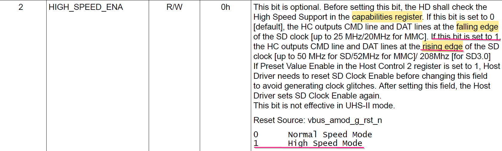
image.png

But on datasheet, the MMC0 High Speed SDR mode transmit on falling edge. 
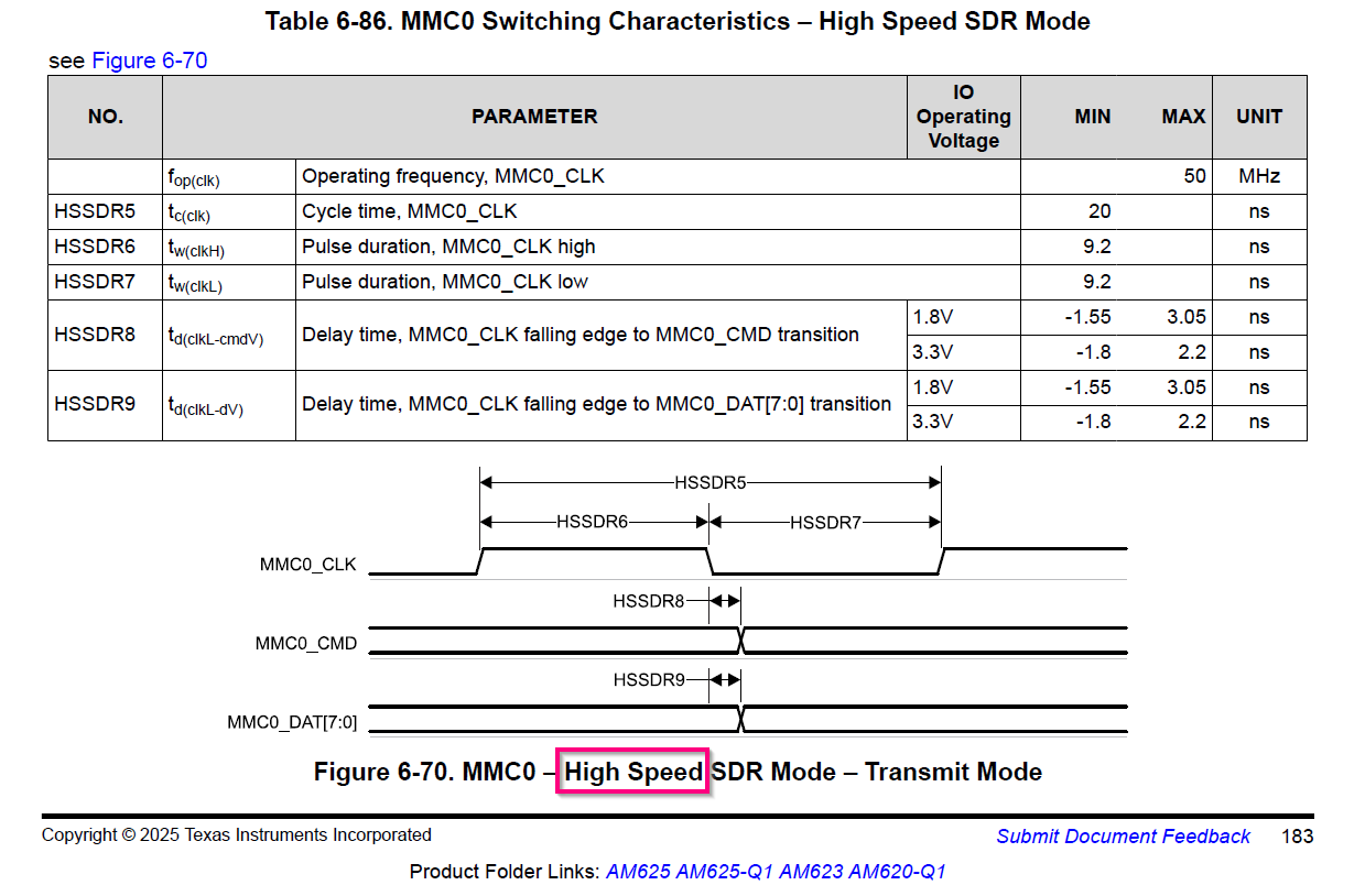
image.png

Is the description wrong, rising edge should corresponding to full cycle timing, or UHS mode.

BTW, how to define the high speed mode?

  • Hello Tony,

    Anastas is currently out of office.

    Please expect a response on 4th May.

    Best Regards,

    Borislav Lazarkov

  • We found it was easier to close MMC0 peripheral timing for High Speed SDR transfers if half-cycle timing was used rather than full-cycle timing. Therefore, we decided to use the same half-cycle data transfer timing approach, where data is changed on the falling edge and captured on the rising edge, for Legacy SDR (up to 25MHz) and High Speed SDR (up to 50MHz).

    There was a plan to include the expected configuration of the following register bits for each supported data transfer mode in the TRM. However, I'm not sure if that was done or still pending.  The data to clock timing is a function of these host controller bits along with the PHY configurations defined in the datasheet "MMC0 DLL Delay Mapping for all Timing Modes" table. 

    MMCSD0_MMC_CTLCFG_HOST_CONTROL1[2] (HIGH_SPEED_ENA),
    MMCSD0_MMC_CTLCFG_HOST_CONTROL2[3,2:0] (V1P8_SIGNAL_ENA, UHS_MODE_SELECT)

    For eMMC on the MMC0 peripheral, the following configuration is expected:

    Legacy SDR        - HIGH_SPEED_ENA = 0b0, V1P8_SIGNAL_ENA = 0b0, UHS_MODE_SELECT = 0x0
    High Speed SDR - HIGH_SPEED_ENA = 0b0, V1P8_SIGNAL_ENA = 0b0, UHS_MODE_SELECT = 0x0
    HS200                  - HIGH_SPEED_ENA = 0b1, V1P8_SIGNAL_ENA = 0b0, UHS_MODE_SELECT = 0x3

    Regards,
    Paul

  • Thanks Paul,

    How do you think the field description of MMCSD0_MMC_CTLCFG_HOST_CONTROL1[2] (HIGH_SPEED_ENA) should be updated? This bit only impacts the data/cmd changing on which clock edge, doesn't matter with clock frequency.  

    Or in other word, on AM62x, it should be set to 1 for UHS mode only for full cycle timing. 

    Or change High Speed Mode to UHS-I mode.

    People usually take the High Speed Mode as 50MHz. 

  • The title of this E2E post seems to indicate you were asking about communication with an eMMC device, which I assume is connected to the AM62x MMC0 port since it is the only port that supports eMMC. If so, none of the UHS data transfer modes associated with MMC0 will apply. The UHS modes only apply when connected to embedded SDIO devices. For the embedded SDIO device UHS use case, we perform data transfers using full-cycle timing.

    The decision to use half-cycle timing for High Speed eMMC communications was done to accommodate older legacy eMMC devices which may have long hold time requirements.

    We still support High Speed data transfers up to 50MHz. However, we perform the data transfers using half-cycle timing rather than full-cycle timing. I agree this may be different than what is expected, but the approach provides better timing margin.

    Regards,
    Paul 

  • Yes, I am talking about eMMC. I understand now.  

    Yes. eMMC0 only support legacy(25MHz), hs(50MHz SDR), and HS200 SDR in dts, while MMC1 and MMC2 support ddr50.

    So eMMC0 only support SDR mode, no matter working on what frequency.

    	sdhci0: mmc@fa10000 {
    		compatible = "ti,am62-sdhci";
    		reg = <0x00 0x0fa10000 0x00 0x1000>, <0x00 0x0fa18000 0x00 0x400>;
    		interrupts = <GIC_SPI 133 IRQ_TYPE_LEVEL_HIGH>;
    		power-domains = <&k3_pds 57 TI_SCI_PD_EXCLUSIVE>;
    		clocks = <&k3_clks 57 5>, <&k3_clks 57 6>;
    		clock-names = "clk_ahb", "clk_xin";
    		bus-width = <8>;
    		mmc-hs200-1_8v;
    		ti,clkbuf-sel = <0x7>;
    		ti,otap-del-sel-legacy = <0x0>;
    		ti,otap-del-sel-mmc-hs = <0x0>;
    		ti,otap-del-sel-hs200 = <0x6>;
    		ti,itap-del-sel-legacy = <0x0>;
    		ti,itap-del-sel-mmc-hs = <0x0>;
    		status = "disabled";
    	};
    	
    	
    	sdhci1: mmc@fa00000 {
    		compatible = "ti,am62-sdhci";
    		reg = <0x00 0x0fa00000 0x00 0x1000>, <0x00 0x0fa08000 0x00 0x400>;
    		interrupts = <GIC_SPI 83 IRQ_TYPE_LEVEL_HIGH>;
    		power-domains = <&k3_pds 58 TI_SCI_PD_EXCLUSIVE>;
    		clocks = <&k3_clks 58 5>, <&k3_clks 58 6>;
    		clock-names = "clk_ahb", "clk_xin";
    		bus-width = <4>;
    		ti,clkbuf-sel = <0x7>;
    		ti,otap-del-sel-legacy = <0x0>;
    		ti,otap-del-sel-sd-hs = <0x0>;
    		ti,otap-del-sel-sdr12 = <0xf>;
    		ti,otap-del-sel-sdr25 = <0xf>;
    		ti,otap-del-sel-sdr50 = <0xc>;
    		ti,otap-del-sel-sdr104 = <0x6>;
    		ti,otap-del-sel-ddr50 = <0x9>;
    		ti,itap-del-sel-legacy = <0x0>;
    		ti,itap-del-sel-sd-hs = <0x0>;
    		ti,itap-del-sel-sdr12 = <0x0>;
    		ti,itap-del-sel-sdr25 = <0x0>;
    		status = "disabled";
    	};
    
    	sdhci2: mmc@fa20000 {
    		compatible = "ti,am62-sdhci";
    		reg = <0x00 0x0fa20000 0x00 0x1000>, <0x00 0x0fa28000 0x00 0x400>;
    		interrupts = <GIC_SPI 82 IRQ_TYPE_LEVEL_HIGH>;
    		power-domains = <&k3_pds 184 TI_SCI_PD_EXCLUSIVE>;
    		clocks = <&k3_clks 184 5>, <&k3_clks 184 6>;
    		clock-names = "clk_ahb", "clk_xin";
    		bus-width = <4>;
    		ti,clkbuf-sel = <0x7>;
    		ti,otap-del-sel-legacy = <0x0>;
    		ti,otap-del-sel-sd-hs = <0x0>;
    		ti,otap-del-sel-sdr12 = <0xf>;
    		ti,otap-del-sel-sdr25 = <0xf>;
    		ti,otap-del-sel-sdr50 = <0xc>;
    		ti,otap-del-sel-sdr104 = <0x6>;
    		ti,otap-del-sel-ddr50 = <0x9>;
    		ti,itap-del-sel-legacy = <0x0>;
    		ti,itap-del-sel-sd-hs = <0x0>;
    		ti,itap-del-sel-sdr12 = <0x0>;
    		ti,itap-del-sel-sdr25 = <0x0>;
    		status = "disabled";
    	};

    So MMCSD0_MMC_CTLCFG_HOST_CONTROL1[2] (HIGH_SPEED_ENA) field description better to be: 

    0: half cycle timing

    1: full cycle timing.

  • Hello Tony, 

    Thank you for the inputs.

    I will check internally and add a JIRA as required.

    Regards,

    Sreenivasa

  • Yes, the register bit description should be updated to avoid any confusion. I will submit a request to update the description.

    Regards,
    Paul