Part Number: TDA4VM
Other Parts Discussed in Thread: DRA829,
Hello Experts,
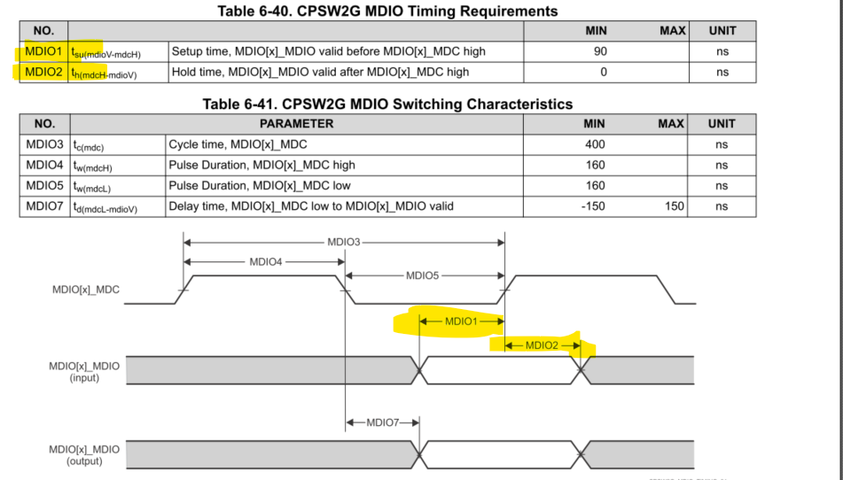
We are using the J721E (DRA829 / TDA4VM / AM68P) processor in conjunction with Marvell Alaska PHY devices (88EA1517 / 88EA1512 and 88E1548P). Currently, I am performing a timing analysis to determine the optimal MDC clock width, taking into account the minimum values of internal delays, setup time, hold time, and clock period.
So far, the analysis has focused on the MDIO write path (CPU to PHY), where the PHY setup and hold time requirements are considered while selecting the MDC timing parameters. However, I would like clarification regarding the MDIO read path (PHY to CPU). Specifically, when data is driven by the PHY and sampled by the processor, should the processor’s MDIO input setup and hold timing requirements, as specified in the processor datasheet, also be included in the timing analysis?
Any additional insights or best practices for MDC clock period selection that account for both read and write paths would be greatly appreciated.
Kind regards
Thank You
Manisha Narayana