Part Number: DRA821U
Other Parts Discussed in Thread: DRA821, SYSCONFIG, TPS6594-Q1
Dear Team,
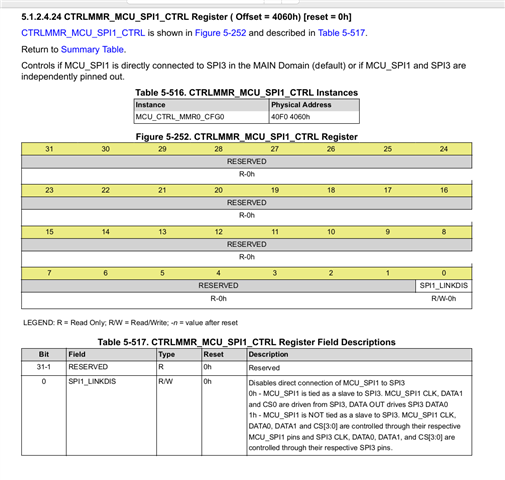
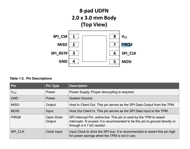
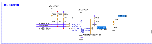
We have connected SRAM (23A512-I/SN) and TPM (ATTPM20P-H6MA1-10) to the MCU SPI1 interface as slave devices on the DRA821U platform and added the corresponding DTSI entries for both devices. In our configuration, SRAM is connected to CS0 and TPM is connected to CS3.
During boot, we observe a timeout error from the TPM driver:
tpm_tis_spi: probe of spi0.3 failed with error -110.
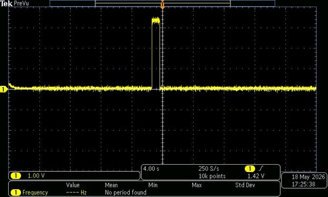
To debug this, we probed the chip select (CS) pin of the SPI controller. We noticed that when the TPM driver is loading, the CS pin does not toggle low. Throughout the entire boot sequence—from U-Boot to kernel—the CS line remains high (as observed on CRO) but the SRAM CS pin is going to low when the SRAM's driver is loading. Also, the clock is generating properly (12.5 MHz).
Additionally, we are facing an issue with the SRAM device where write operations to the memory block are not functioning as expected.
Could you please guide us on how to resolve these issues? Also, is there any limitation or special consideration for using multiple chip select lines on MCU SPI?
SDK Version: 09.02.00.04
Yocto: Kirkstone
SoC: DRA821
pin mux
-------------
| Interface | Functionality | Pad name | Pin No | GPIO No | Input/Output |
| SRAM | SPI_B_SDO | MCU_SPI1_D0/WKUP_GPIO0_1 | B19 | - | Output |
| SPI_B_SDI | MCU_SPI1_D1/WKUP_GPIO0_2 | D14 | - | Input | |
| SPI_B_HOLD | MCU_OSPI0_DQS/MCU_HYPERBUS0_RWDS/WKUP_GPIO0_18 | B7 | - | Output | |
| SPI_B_CS0# | MCU_SPI1_CS0/WKUP_GPIO0_3 | B21 | - | Output | |
| SPI_B_SCK | MCU_SPI1_CLK/WKUP_GPIO0_0 | B18 | - | Output | |
| SPI_B_WP | MCU_OSPI0_CSN3/MCU_HYPERBUS0_INTN/MCU_HYPERBUS0_WPN/MCU_OSPI0_RESET_OUT1/MCU_OSPI0_ECC_FAIL/WKUP_GPIO0_31 | D5 | - | Output | |
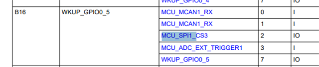
| TPM Module | SPI_B_CS1#(GPIO_A_7) | MCU_MCAN1_RX/MCU_SPI1_CS3/MCU_ADC_EXT_TRIGGER1/WKUP_GPIO0_5 | B16 | GPIO0_5 | Output |
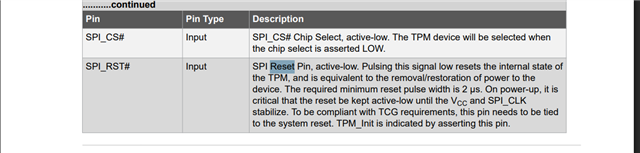
| TPM_RSTn(GPIO_A_5) | SPI0_CS0/UART0_CTSN/GPIO0_51 | W3 | GPIO0_51 | Output | |
| SPI_B_SCK | MCU_SPI1_CLK/WKUP_GPIO0_0 | B18 | GPIO0_0 | Output | |
| SPI_B_SDO | MCU_SPI1_D0/WKUP_GPIO0_1 | B19 | GPIO0_1 | Output | |
| SPI_B_SDI | MCU_SPI1_D1/WKUP_GPIO0_2 | D14 | GPIO0_2 | Input |
DTSI Entry
------------------
&mcu_spi1 {
status = "okay";
pinctrl-names = "default";
pinctrl-0 = <&spi_pins_default>;
ti,spi-num-cs = <4>;
spi-sram@0 {
compatible = "microchip,mchp23a512";
reg = <0x0>;
spi-max-frequency = <20000000>;
#address-cells = <1>;
#size-cells = <1>;
status = "okay";
};
tpm@3{
compatible = "tcg,tpm_tis-spi";
reg = <0x3>;
spi-max-frequency = <16000000>;
reset-gpios = <&main_gpio0 51 GPIO_ACTIVE_HIGH>;
#address-cells = <1>;
#size-cells = <1>;
status = "okay";
};
};
&wkup_pmx2 {
spi_pins_default: spi-pins-default {
pinctrl-single,pins = <
J721E_WKUP_IOPAD(0x58, PIN_INPUT, 0) /* (B18) WKUP_GPIO0_0.MCU_SPI1_CLK */
J721E_WKUP_IOPAD(0x5c, PIN_OUTPUT, 0) /* (B19) WKUP_GPIO0_1.MCU_SPI1_D0 */
J721E_WKUP_IOPAD(0x60, PIN_INPUT, 0) /* (D14) WKUP_GPIO0_2.MCU_SPI1_D1 */
J721E_WKUP_IOPAD(0x64, PIN_OUTPUT, 0) /* (B21) WKUP_GPIO0_3.MCU_SPI1_CS0 */
J721E_WKUP_IOPAD(0x06c, PIN_OUTPUT, 0) /* (B16) WKUP_GPIO0_5 TPM CS*/
>;
};
};
We would appreciate your guidance in resolving the TPM probe failure and SRAM write issue.
Thanks and Regards,
Subashini