


Part Number: J721EXCPXEVM
Other Parts Discussed in Thread: DRA829
Dear TI Team,
I am currently encountering an issue while using the DRA829 device.
My system is configured with 4GB DDR memory, and I need to enable DDR ECC using the MSMC2DDR bridge inline ECC feature.
From the SoC point of view, the DDR address space is divided into two regions:
-
Low DDR region:
0x80000000 ~ 0xFFFFFFFF
-
High DDR region:
0x880000000 ~ 0x8FFFFFFFF
At present, I am able to successfully inject and trigger ECC errors within the lower 2GB DDR address region from the C7x core.
However, I am unable to trigger ECC errors within the upper 2GB DDR address region.
Could you please help explain why this happens?
Thank you very much for your support.
My ECC configuration is as follows, I have already initialized the DDR memory space using UDMA,
and reserved 1/9 of the DDR space for ECC parity storage:
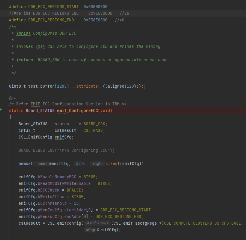
The code used to trigger ECC errors in the high DDR address region on the C7x core is shown below:
{
volatile uint64_t *gTest_Addr = NULL; volatile uint64_t testVal; volatile uint64_t testVal2; volatile uint64_t *translatedMemPtr;
/* Clear any residual ECC errors */ DDR_clearAllECCError();
/* Inject error */ gTest_Addr = (uint64_t *) ((0x880000000));
/* Write back any pending writes */ CacheP_wbInv ((void *)gTest_Addr, 4);
/* Read value from test location */ testVal = gTest_Addr[0];
/* Flip one bit to introduce error */ testVal2 = testVal ^ 0x00010000u;
/* Calculate translated address */ translatedMemPtr = (volatile uint64_t *)(DDRGetTranslatedAddress((uintptr_t)gTest_Addr));
/* Generating a 1b ECC error */ /* NOTE: The following section should NOT be useed in actual application */ /* ================================================================================ */
/* Temporarily disable ECC */ CSL_emifDisableECC ((CSL_emif_sscfgRegs *)CSL_COMPUTE_CLUSTER0_SS_CFG_BASE);
/* Now corrupt the value */ *(translatedMemPtr) = testVal2; CacheP_wbInv ((void *)translatedMemPtr, 4);
/* Enable back ECC */ CSL_emifEnableECC ((CSL_emif_sscfgRegs *)CSL_COMPUTE_CLUSTER0_SS_CFG_BASE);
/* ================================================================================ */
/* Invalidate cache */ CacheP_Inv ((void *)gTest_Addr, 4);
/* Read value to trigger error */ testVal2 = gTest_Addr[0];
}
#define EMIF_ECC_MEM_BLOCK_SIZE 0x200#define EMIF_ECC_DATA_SIZE_PER_BLOCK 0x40uintptr_t DDRGetTranslatedAddress(uintptr_t memAddress){ uint64_t memIndex; uintptr_t translatedMemAddr;
memIndex = (memAddress-0x880000000u)/EMIF_ECC_MEM_BLOCK_SIZE; if ((memIndex & 0x1u) == 0) { translatedMemAddr = memAddress + ((memIndex)*EMIF_ECC_DATA_SIZE_PER_BLOCK); } else { translatedMemAddr = memAddress + ((memIndex+1u)*EMIF_ECC_DATA_SIZE_PER_BLOCK); } return translatedMemAddr;}
Could you please let me know if there is anything wrong with my procedure or configuration?
