This thread has been locked.

If you have a related question, please click the "Ask a related question" button in the top right corner. The newly created question will be automatically linked to this question.

old uboot.bin worked well in SEED-DEC137(same as EVM137) doesn't work in new designed OMAPL137 board.

Here are is the history of our purchasing:
    1    Bought SEED-DEC137 which is based on EVM137 of yours and SDS510 JTAG EMULATOR from SEEDdsp in 2009.
          Everything goes fine.

    2    Bought a batch of OMAPL137 from ARROWasia in 2011.7, designed our board based on SEED-DEC137.
          Our new board pass all the test under CCS3.3(NAND,SDRAM etc), but the board doesn't work in nand mode after reset, and there is no message from UART2.
 
 Here is our analysis:
    we find out thae the ROM ID in OMAPL137 of SEED-DEC137 is D800K001, and the ROM ID in OMAPL137 we bought from ARROWasia is D800K003, so maybe the problem comes from chip difference?
 
 Here is the procedures of our boot case:
    1    change the OMAPL137 pin to nand flash boot mode
    2    we take the same u-boot.out used in SEED-DEC137
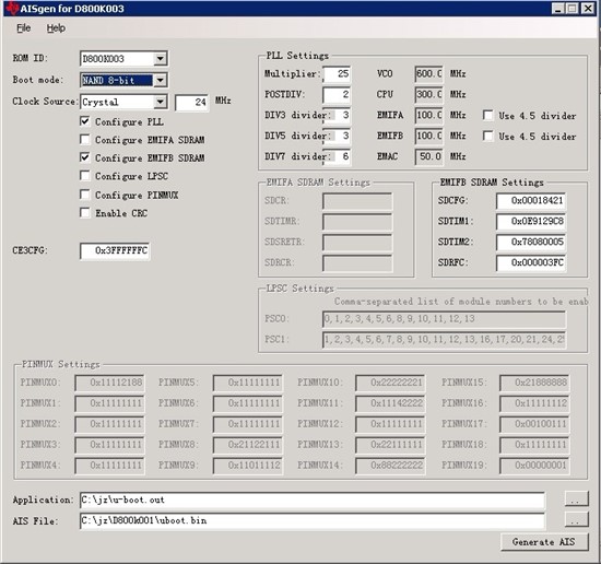
    3    take new downloaded AISgen for D800K003 to generate uboot.bin from the u-boot.out
    4    take CCS3.3 to load nandwrite project in "OMAP_L137_example" which is used in SEED-DEC137 nand flash burning, burn the uboot.bin into our board.
    5    after nandwrite successfully finished burning, quit the CCS3.3, reset the board, nothing happenned, and
there is no message from UART.
 
 The problem delayed our project for several monthes, so please give us some effective consultation and help.
  • this is the configuration of AISGen for D800K003 I used to generate uboot.bin, by the way ,the u-boot.out works well in AISGen with D800K001 in SEED-DEC137(EVM137)

  • ---------------------------------------------
    |             Device Information            |
    ---------------------------------------------
    DEV_INFO_00 = 0x9B7DF02F
    DEV_INFO_01 = 0x00000000
    DEV_INFO_02 = 0x0000FB7F
    DEV_INFO_03 = 0x00000022
    DEV_INFO_04 = 0x00000000
    DEV_INFO_05 = 0x000003E0
    DEV_INFO_06 = 0x00000080
    DEV_INFO_07-DEV_INFO_08-DEV_INFO_09-DEV_INFO_10-DEV_INFO_11-DEV_INFO_12 = 8-0-152606-21-22-23
    DEV_INFO_13,DEV_INFO_14,DEV_INFO_15,DEV_INFO_16 = 0,0,0,5293
    -----
    DEV_INFO_17 = 0x00030003
    DEV_INFO_18 = 0x00000000
    DEV_INFO_19 = 00000
    -----
    DEV_INFO_20 = 0x30303864
    DEV_INFO_21 = 0x3330306B
    DEV_INFO_22 = 0x00000000
    DEV_INFO_23 = 0x00000000
    -----
    DEV_INFO_24 = 0x15017016
    DEV_INFO_25 = 0x0802541E
    DEV_INFO_06 = 0x00000080
    DEV_INFO_26 = 0x295A0000
    
    
    ---------------------------------------------
    |               BOOTROM Info                |
    ---------------------------------------------
    ROM ID: d800k003 
    Silicon Revision 2.0
    Boot pins: 64383
    Boot Mode: NAND 8 (0x0000FB7F)
    
    ROM Status Code: 0x00000000 
    Description: No error
    
    Program Counter (PC) = 0xC82DAE28
    
    ---------------------------------------------
    |              Clock Information             |
    ---------------------------------------------
    
    PLLs configured to utilize crystal.
    ASYNC3 = PLL0_SYSCLK2
    
    NOTE:  All clock frequencies in following PLL sections are based
    off OSCIN = 24 MHz.  If that value does not match your hardware
    you should change the #define in the top of the gel file, save it,
    and then reload.
    
    ---------------------------------------------
    |              PLL0 Information             |
    ---------------------------------------------
    
    PLL0_SYSCLK1 = 300 MHz
    PLL0_SYSCLK2 = 150 MHz
    PLL0_SYSCLK3 = 100 MHz
    PLL0_SYSCLK4 = 75 MHz
    PLL0_SYSCLK5 = 50 MHz
    PLL0_SYSCLK6 = 300 MHz
    PLL0_SYSCLK7 = 37 MHz
    
    ---------------------------------------------
    |              PSC0 Information             |
    ---------------------------------------------
    
    State Decoder:
     0 = SwRstDisable (reset asserted, clock off)
     1 = SyncReset (reset assered, clock on)
     2 = Disable (reset de-asserted, clock off)
     3 = Enable (reset de-asserted, clock on)
    >3 = Transition in progress
    
    Module 0:	EDMA3CC (0)        STATE = 3
    Module 1:	EDMA3 TC0          STATE = 3
    Module 2:	EDMA3 TC1          STATE = 3
    Module 3:	EMIFA (BR7)        STATE = 3
    Module 4:	SPI 0              STATE = 3
    Module 5:	MMC/SD 0           STATE = 3
    Module 6:	AINTC              STATE = 3
    Module 7:	ARM RAM/ROM        STATE = 3
    Module 9:	UART 0             STATE = 3
    Module 10:	SCR 0 (BR0/1/2/8)  STATE = 3
    Module 11:	SCR 1 (BR4)        STATE = 3
    Module 12:	SCR 2 (BR3/5/6)    STATE = 3
    Module 13:	PRUSS              STATE = 3
    Module 14:	ARM                STATE = 3
    Module 15:	DSP                STATE = 3
    
    ---------------------------------------------
    |              PSC1 Information             |
    ---------------------------------------------
    
    State Decoder:
     0 = SwRstDisable (reset asserted, clock off)
     1 = SyncReset (reset assered, clock on)
     2 = Disable (reset de-asserted, clock off)
     3 = Enable (reset de-asserted, clock on)
    >3 = Transition in progress
    
    Module 1:	USB0 (2.0)         STATE = 3
    Module 2:	USB1 (1.1)         STATE = 3
    Module 3:	GPIO               STATE = 3
    Module 4:	UHPI               STATE = 3
    Module 5:	EMAC               STATE = 3
    Module 6:	EMIFB (BR20)       STATE = 3
    Module 7:	MCASP0 + FIFO      STATE = 3
    Module 8:	MCASP1 + FIFO      STATE = 3
    Module 9:	MCASP2 + FIFO      STATE = 3
    Module 10:	SPI 1              STATE = 3
    Module 11:	I2C 1              STATE = 3
    Module 12:	UART 1             STATE = 3
    Module 13:	UART 2             STATE = 3
    Module 16:	LCDC               STATE = 3
    Module 17:	eHRPWM (all)       STATE = 3
    Module 20:	eCAP (all)         STATE = 3
    Module 21:	eQEP 0/1           STATE = 3
    Module 24:	SCR8 (Br15)        STATE = 3
    Module 25:	SCR7 (Br12)        STATE = 3
    Module 26:	SCR12 (Br18)       STATE = 3
    Module 31:	L3 RAM (Br13)      STATE = 3
    

    this is the diagnostics comes out with OMAPL1x_debug.gel in CCS3.3