


looking at the last SPRABI2B from March 2012.
I need some advise about HyperLink routing recommendations.
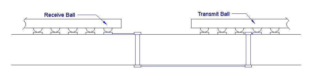
There is a request to route the Differential pairs as microstrip on external layers - i quote :
"To prevent crosstalk in a simple board stack-up, we recommend that the
differential receive pairs be routed as microstrip (outer layer) on one side of the
board and the differential transmit pairs be routed as microstrip (outer layer) on
the other side of the board."
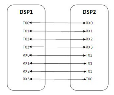
Since the Hyperlink connectivity is between 2 DSP's and Hyperlink BGA pins are spread in external and internal BGA rows
and TX is connected to RX.
If you start routing on external layer top from BGA pins on rows 1 or 2 ( BGA is mounted on TOP ) to connect to the second BGA pins you need to reach pins in row 4 and 5
Question 1 ) Can you explain how can this accomplished - do you have a Reference design that complies to this request ?
Question 2) what do you mean by "simple board stack-up" my boards will be about 18 layers with 9 PWR/GND layers - how is it related to the routing of hyperlink?
Question 3) In case of routing in internal layer what is the maximum allowed stub of via without backdrilling and without using blind/buried vias
I found a reference -i quote "In high-speed designs, a good rule of thumb to remember is that a via stub should be less than 300mils/BR in length; where BR is the bit rate in Gb/s." can be found at http://blog.lamsimenterprises.com/
If this rule of thumb is correct - can i allow a stub of 300/12.5=24mils=0.6mm ?
Question 4) Impedance control ( PCB manufacturing variations ) on external layers is not as good in internal layers .
is the hyperlink sensitive to larger impedance variations along the transmission line - my routing length can be up to 4" ?
Question 5) About signal losses:
is there any loss budget associated with the hyperlink? do you recommend using lower loss matrials/high speed materials ?
In Extrenal layer traces skin effect problem is greater relative to stripline since of the fact that current preffers flowing adjacent to a reference plane
stripline has 2 reference planes while microstrip has only one?
Question 6) you recommend using a GND via near each location the hyperlink changes layer
Regarding the loss due to impedance discontinuity :
vias characteristic impedance is lower than 50 ohm - do you recommend trying to increase/control the via impedance ?
by lowering via capacitance achived by increasing clearance to planes and eliminating few internal via pads.
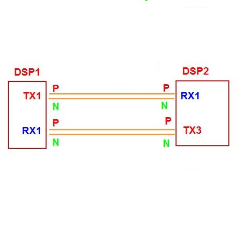
Question 7 ) for ease of routing :i understand that all 4 lanes diff pairs can be swapped ( maintanig pairing) and also each pair can be swapped between P an N
can i freely mix between all 8 diff pairs ?
question 8 ) loosley coupled differntial pairs decrease losses caused by skin effect while can increase material losses ( loss tangent)
what is the recommended/optimal differntial coupling ( or trace width and trace clearance )?
question 9) what is the recommended spacing between pairs and other signals ? what is the minimum for short distances?
Cheers,
Roby


