This thread has been locked.

If you have a related question, please click the "Ask a related question" button in the top right corner. The newly created question will be automatically linked to this question.

AM335x MMU Not Working

Other Parts Discussed in Thread: SYSBIOS, AM3359

I am working on getting MMU working on AM335x, we have our own custom board (closer design to Beagleboard) with NAND flash

i am able to boot from NAND flash, now i want to use MMU in my code, i am using Codesourcery GCC ver 4.2.3 to compile my own written standalone code

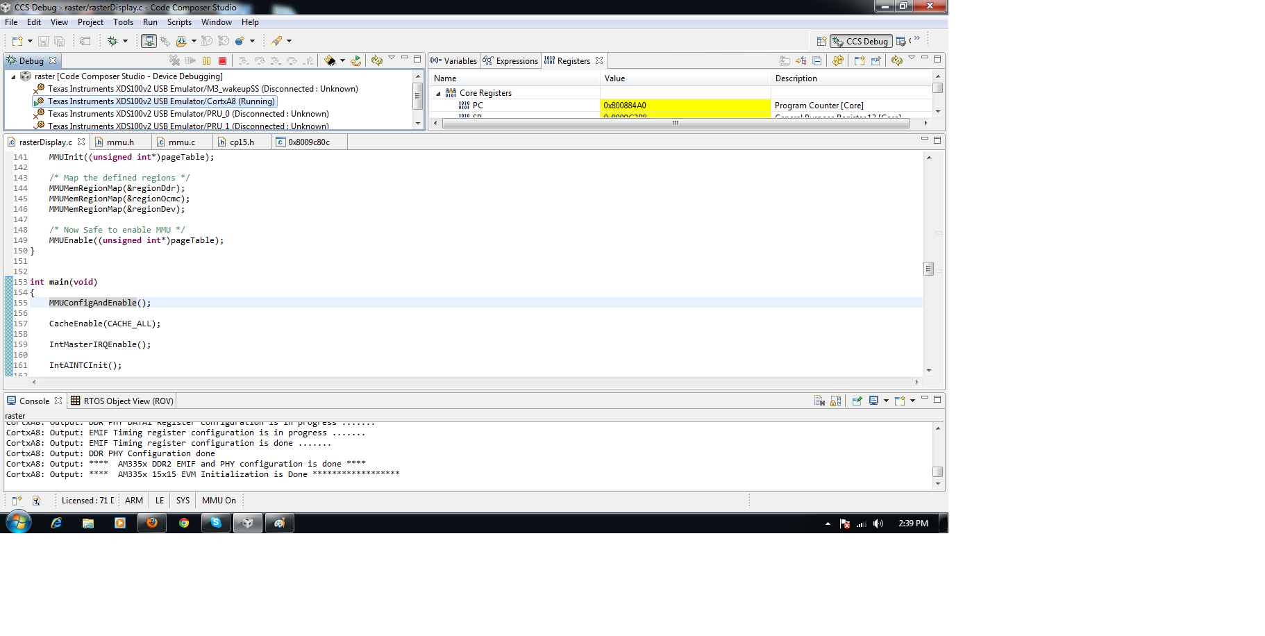
i have used MMU code from Starterware (ver 02.00.00.06) code, but my code stops executing after CP15MMUEnable(); i have used all same code from starterware for MMU, i have verified pageTable address and also verified that entries in pageTable are correct

My code boots from NAND flash, then i copy my initial bootloader to DDR2 RAM at address 0x80000000 and then jump DDR2 for execution, (i want to enable MMU for whole DDR2 memory region) there are certain messages i sent to terminal through UART0, and my code boots up preoperly, but when i try to enable MMU, at CP15MMUEnable, it halts and does not send the characters to terminal after this instruction, am i doing something wrong?

My MMU pageTable address is at 0x83904000 which is 16K boundary aligned as instructed

Below is the code patch i am using to enable MMU, which is taken from starterware code

/*
** Function to setup MMU. This function Maps three regions ( 1. DDR
** 2. OCMC and 3. Device memory) and enables MMU.
*/
void MMUConfigAndEnable(void)
{
/*
** Define DDR memory region of AM335x. DDR can be configured as Normal
** memory with R/W access in user/privileged modes. The cache attributes
** specified here are,
** Inner - Write through, No Write Allocate
** Outer - Write Back, Write Allocate
*/
REGION regionDdr = {
MMU_PGTYPE_SECTION, START_ADDR_DDR, NUM_SECTIONS_DDR,
MMU_MEMTYPE_NORMAL_NON_SHAREABLE(MMU_CACHE_WT_NOWA,
MMU_CACHE_WB_WA),
MMU_REGION_NON_SECURE, MMU_AP_PRV_RW_USR_RW,
(unsigned int*)pageTable
};
/*
** Define OCMC RAM region of AM335x. Same Attributes of DDR region given.
*/
REGION regionOcmc = {
MMU_PGTYPE_SECTION, START_ADDR_OCMC, NUM_SECTIONS_OCMC,
MMU_MEMTYPE_NORMAL_NON_SHAREABLE(MMU_CACHE_WT_NOWA,
MMU_CACHE_WB_WA),
MMU_REGION_NON_SECURE, MMU_AP_PRV_RW_USR_RW,
(unsigned int*)pageTable
};

/*
** Define Device Memory Region. The region between OCMC and DDR is
** configured as device memory, with R/W access in user/privileged modes.
** Also, the region is marked 'Execute Never'.
*/
REGION regionDev = {
MMU_PGTYPE_SECTION, START_ADDR_DEV, NUM_SECTIONS_DEV,
MMU_MEMTYPE_DEVICE_SHAREABLE,
MMU_REGION_NON_SECURE,
MMU_AP_PRV_RW_USR_RW | MMU_SECTION_EXEC_NEVER,
(unsigned int*)pageTable
};

/* Initialize the page table and MMU */
MMUInit((unsigned int*)pageTable);

/* Map the defined regions */
MMUMemRegionMap(&regionDdr);
MMUMemRegionMap(&regionOcmc);
MMUMemRegionMap(&regionDev);

/* Now Safe to enable MMU */
MMUEnable((unsigned int*)pageTable);
}

void MMUInit(unsigned int *masterPt)
{
unsigned int idx;

/* Invalidate the TLB entries */
CP15TlbInvalidate();

/* Set domain access rights */
CP15DomainAccessClientSet();

/* Disable TEX remapping, Access Flag usage and alignment check */
CP15ControlFeatureDisable( CP15_CONTROL_TEXREMAP
| CP15_CONTROL_ACCESSFLAG
| CP15_CONTROL_ALIGN_CHCK
| CP15_CONTROL_MMU);

/* Configure the TTB Control register to use only TTB0 */
CP15TtbCtlTtb0Config();

/* Se the master page table with fault entries */
for(idx = MMU_PAGETABLE_NUM_ENTRY; idx !=0; idx--)
{
*masterPt++ = MMU_PAGETABLE_ENTRY_FAULT;
}
}

void MMUMemRegionMap(REGION *region)
{
unsigned int *ptEntryPtr;
unsigned int ptEntry;
int idx;

/* Get the first entry in the page table to set */
ptEntryPtr = region->masterPtPtr +
(region->startAddr >> MMU_PAGEBOUND_SHIFT);

/* Set the pointer to the last entry */
ptEntryPtr += (region->numPages - 1);

/* Get the start Address MSB 3 nibbles. Ignore extended address */
ptEntry = (region->startAddr & region->pgType) & MMU_PGADDR_MASK;

/*
** Update the page table entry with memory attributes and
** Access Permissions and Security.
** All the regions will be marked as global.
*/
ptEntry |= ((MMU_PGTYPE_MASK & region->pgType)
| region->accsCtrl | region->memAttrib
| region->secureType);

/* Set the entries in the page table for the region attributes */
for(idx = (region->numPages - 1); idx >= 0; idx--)
{
*ptEntryPtr-- = ptEntry + (idx << MMU_PAGEBOUND_SHIFT) ;
}
}

void MMUEnable(unsigned int *masterPt)
{
/* Set TTB0 register */
CP15Ttb0Set((unsigned int)masterPt);

/* Enable MMU */
CP15MMUEnable();
}

Please help !!!

  • Hi Alankar,

    The sequence you mentioned seems to be OK. Could you please check if the macro NUM_SECTIONS_DDR is given proper value ?

    Is the code aborting when you execute MCR instruction in CP15MMUEnable()?


    Regards,

    Sujith.

  • Hi Sujith,

    thanks for looking into this...

    value for macro NUM_SECTIONS_DDR is 512, i also tried with value as 2, but same results

    and you are right, the code aborts when it execute  " MCR     p15, #0, r0, c1, c0, #0 " instruction, when i comment this instruction the code executes well as it doesn't  enable MMU this time.

    Also code is executing in system mode, so there should be no any issue in accessing CP15 register..

    Alankar

  • Hi Alankar,

    The value 512 should be okay then. What is the address of the instruction "MCR     p15, #0, r0, c1, c0, #0 " ? I hope you have verified the corresponding page table data.

    Also, have you made sure that no Cache/MMU was enabled before executing this ?

    Just before enabing the MMU, can you please read the TTB0 register using "MRC     p15, #0, r0, c2, c0, #0"  and verify it is page table address?

    Regards,

    Sujith

  • Hi Sujith,

    Sorry but i couldn't get your first point, as per my understanding address of instruction means you are asking about where this instruction is mapped in code, if my understanding is right, address of this instruction is 0x80001b40, this is in first MB page of DDR2 RAM, page table data corresponding to this page is 0x80095c0a

    all 512 pages of DDR2 ram configured in page table with the attributes as in my first post, is it ok that i am assigning attributes to the page from where i am executing? i think it should be ok, i used in this fashion in some of my older codes with ARM926ejs core (i think arm mmu v4), so this should not be an issue

    Also i am sure that no Cache/MMU are enabled before executing this code, in my main, i am initializing all PLLs (initialized to run @720MHz TURBO mode), initialize UART0 to send characters to terminal and then i call MMUConfigAndEnable(); function (as posted in my first post)... but it halts at MMU enable instruction

    As you asked, i just read the TTB0 register before enabling MMU and it has the right value of page table address (currently 0x8390c000 page table address changed from my first post as i made it static)

    I tried further, and now i have written a small piece of code which i can download to AM335x through XMODEM and can directly execute (Do not boot from NAND flash), now in this code, i have initialized the PLLs, DDR2, UART0 and then MMUConfigAndEnable(); still no luck... Again in same code no PLL init, no DDR init, no UART0 init, directly MMUConfigAndEnable(); still same issue

    i am really not getting, whats going wrong...

    regards,

    Alankar

  • Hi Alankar,

    I dont see any problem in your configurations. From your posts, everything seems to be proper. Since the page table is also set and the TTB0 register is also written  correctly, I am confused why the abort is happening !  May be we can try to analyze the type of exception getting generated.

    Meanwhile I will try to see other possibilities for the abort to be generated (I am not able to reproduce this unfortunately..). If possible, can you share your init code ? ( Just to see after the ROM code hands over the control to your Boot Loader and application,  what all ARM core related changes you are making compared to StarterWare)

    Regards,

    Sujith.

  • Hi Sujith,

    i am also confused now, and totally stuck, i tried lot different thing still no luck, i will try to analyze which type of exception is getting generated

    Here is my init code and its flow

    at reset i call Reset_Handler as follows

    .EQU Mode_USR, 0x10
    .EQU Mode_FIQ, 0x11
    .EQU Mode_IRQ, 0x12
    .EQU Mode_SVC, 0x13
    .EQU Mode_ABT, 0x17
    .EQU Mode_UND, 0x1B
    .EQU Mode_SYS, 0x1F /*; available on ARM Arch 4 and later*/

    .EQU I_Bit, 0x80 /* when I bit is set, IRQ is disabled*/
    .EQU F_Bit, 0x40 /* when F bit is set, FIQ is disabled*/

    /*; --- Amount of memory (in bytes) allocated for stacks*/


    .EQU Len_FIQ_Stack, 0
    .EQU Len_IRQ_Stack, 1024
    .EQU Len_ABT_Stack, 0
    .EQU Len_UND_Stack, 0
    .EQU Len_SVC_Stack, 1024
    .EQU Len_USR_Stack, 4096
    .EQU Len_SYS_Stack, 0

    /*
    ; Add lengths >0 for FIQ_Stack, ABT_Stack, UND_Stack if you need them.
    ; Offsets will be loaded as immediate values.
    ; Offsets must be 8 byte aligned.
    */
    .EQU Offset_FIQ_Stack, 0
    .EQU Offset_IRQ_Stack, Offset_FIQ_Stack + Len_FIQ_Stack
    .EQU Offset_ABT_Stack, Offset_IRQ_Stack + Len_IRQ_Stack
    .EQU Offset_UND_Stack, Offset_ABT_Stack + Len_ABT_Stack
    .EQU Offset_SVC_Stack, Offset_UND_Stack + Len_UND_Stack
    .EQU Offset_USR_Stack, Offset_SVC_Stack + Len_SVC_Stack
    .EQU Offset_SYS_Stack, Offset_USR_Stack + Len_USR_Stack

    .global Reset_Handler

    .extern __main

    Reset_Handler:

    /*; --- Initialize stack pointer registers

    ; Enter each mode in turn and set up the stack pointer*/

    /*IMPORT top_of_stacks ; defined in stack.s and located by scatter file*/

    .equ top_of_stacks, 0x40300000


    LDR r0, =top_of_stacks

    MSR CPSR_c, #Mode_FIQ|I_Bit|F_Bit
    SUB sp, r0, #Offset_FIQ_Stack

    MSR CPSR_c, #Mode_IRQ|I_Bit|F_Bit
    SUB sp, r0, #Offset_IRQ_Stack

    MSR CPSR_c, #Mode_ABT|I_Bit|F_Bit
    SUB sp, r0, #Offset_ABT_Stack

    MSR CPSR_c, #Mode_UND|I_Bit|F_Bit
    SUB sp, r0, #Offset_UND_Stack


    /*
    ;--------------------------------------------------------------------------
    ; MS RECOMMENDATION:
    ; Put the processor in supervisor mode
    ; Disable the interrupt request (IRQ) and fast interrupt request (FIQ)
    ; inputs
    ;--------------------------------------------------------------------------
    */

    MSR CPSR_c, #Mode_SVC|I_Bit|F_Bit
    SUB sp, r0, #Offset_SVC_Stack

    /* Enable interrupt and put processor into system mode */

    MSR CPSR_c, #Mode_SYS|F_Bit
    SUB sp, r0, #Offset_USR_Stack


    b __main


    then it jumps to __main function, where i do all global initialized and uninitialized variable initilization, code for __main is as follows


    void __main()
    {
    extern char end, _data, _edata, _bstart, _bend;

    //extern char _source, _deststart, _destend;
    char *src,*dst;


    /*clearing ram for firmware*/
    for(dst = (char *)&_bstart;dst< &_bend;dst++)
    *dst=0;

    src = &end; // src = end address of code & starting address of .data
    dst = &_data; // dst = starting address of ram where the .data will be loaded

    /* firmware data copying into ram */
    while (dst < &_edata)
    {
    *dst++ = *src++;
    }


    main();

    }


    after this i call upon main() function, where i first init UART0 and then call MMUConfigAndEnable();, below is the code for function main();


    UART_InitCom1();    // initialize UART0

    LOG("_boot-block_");     // Function to send string to UART0

    MMUConfigAndEnable();

    LOG("\n MMU Enabled");     // Function to send string to UART0


    I could see first log on terminal, but code aborts at MMUConfigAndEnable(). and i could not see the next log


    regards,

    Alankar


  • Hi Alankar,

    Can we disable IRQs before calling MMUConfigAndEnable() and Reenable IRQ after that ?

    like, 

       MasterIRQDisable(); // IRQ disabling in CPSR

       MMUConfigAndEnable(); //

       LOG("\n MMU Enabled"); //   ONLY if UART Print is not interrupt based.

      MasterIRQEnable();  // Reenable in CPSR

    With this, we will try to avoid any IRQ related things coming into picture. (As you know, ideally it shouldnt happen. But some other platform, I remember I was mislead with an abort at an ADD instruction because of some IRQ related configurations.. so lets isolate it)

    You can comment "LOG("\n MMU Enabled")" if the LOG is interrupt based.

    With the above changes, can we check if the abort is generated at the same MCR instruction which is enabling MMU ?

    Regards,

    Sujith.

  • Hi Sujith,

    Just checked with disabling IRQ at CPSR, but no luck...

    Actually LOG is not interrupt based, and i have not used any interrupt in this code yet, so i just disabled the IRQ in init as follows

    MSR CPSR_c, #Mode_SYS|F_Bit|I_Bit
    SUB sp, r0, #Offset_USR_Stack


    still the abort is generated at same MCR instruction which enables the MMU


    Regards,

    Alankar

  • Hi Sujith,

    Finally i got MMU working in my code, the issue was, there was a default FAULT entry added for internal RAM region, and my stack memory was located in internal memory, so i added page table entry for internal RAM region and it worked...

    but after this i couldnt see performance difference after enabling MMU, i seen one of queries on e2e, and i found that i need to make DDR region as MMU_MEMTYPE_NORMAL_NON_SHAREABLE, after this modifications i could see 30x performance, that was really great...

    now i moved forward with my original bootloader, which has LCD interface, NAND flash interface, UART0 and some other GPIOs, i enabled MMU in this bootloader also, but i seen very strange behavior in lot of cases, my code got stuck at one place where i configure one GPIO pin to turn on LED on it, i added some delay before writing to GPIO_OE register and this time it does not stuck (very strange), now i have some characters displayed on screen (which was getting displayed properly before MMU enabled) now there is lot garbage data i see on LCD, so same code does not work after MMU enabled, so i made LCD RAM buffer area page as MMU_MEMTYPE_NORMAL_SHAREABLE and then i see proper characters on LCD, now i have NAND flash write function which was working properly before MMU enabled and now after MMU enabled its getting stuck in between, i tried further on this and i found that when i enable DCACHE then i see such type of issues, if i enable only ICACHE, i dont see lot of issues (still there are some, and i have to compromise on performance which i dont want), but after enabling D and I CACHE, its forcing me to debug a lot to workout my original code which was previously working, and i am not comfortable in adding delays at some places and get it to work

    I have not worked too deep with MMU, and in our product we do not have any operating system, we have our own os written in some sort of assembly and C, am i missing something while configuring the MMU, do i need to do cache flush or such sort of operations in code. i didnt see such major issues with old MMU (with ARM926ejs)

    i am really facing such lot issues with my working code after the MMU is enabled, Can you please help me with this, i am really confused now

    Alankar

  • Hi Alankar,

    Great.. At last you got MMU working. But I am surprised why it should abort in the MCR instruction. Anyway, now we got it working..

    And, with LCD, I hope you are using EDMA. Hence, you will have to do Cache Maintanance operations if the memory is NON SHAREABLE. Also, you have to make sure that all the buffers on which DMA is performed, are cache-line aligned (in Cortex A8 its 64 byte) and the buffer size is multiple of 64 byte.

    Even if you clean/flush correctly, and you dont align the buffers properly, it may give other side effects.

    You can download the latest StarterWare 02.00.00.07 release and refer to EVM-SK examples  for the same.

    Regards,

    Sujith.

  • hello,I am also come with same problem in nand read/write.

    when I only turn the I-cache on , the operation to read/write nand flash work goes well . but if i turn on the D-cache . Nand read is  ok ,but write stops unreasonable. 

    the question is :

    > if i turn on the D-cache , what should i do to solve the problem?

  • Hi, 

    When you turn the D-Cache On, you should make sure that cache operations are performed. Regarding Cache and Cache maintanance operations, you can refer to ARM Architecture Reference Manual. Also the EVM-SK examples in StarterWare 02.00.00.07 demonstrates cache maintanance operations.

    Regards,

    Sujith.

  • thanks!I am confused about : 

    > what's the main difference between evmskAM335x and evmAM335x ?

  • Hi,

    EVM-SK is a low cost board, with smaller LCD display, two ethernet ports etc. However, NAND is not available. I hope you are using EVM. However, you can refer to EVM-SK examples if you need to know how cache operations are performed.

    Regards,

    Sujith

  • YES. I'm using the EVM.

    I'll try that way.

  • I am getting stuck in the cache problem now!

    The problem is writing the nand flash .  I am using am335xEVM board. And I use the nandlib in the starterware AM335X_StarterWare_02_00_00_07. 

    When i turn on the cache with the CacheEnable(CACHE_ALL) function , the nand write process get stuck in the functiong NANDDataWrite(). So I clean the cache to make a buffer in D-Cache to be coherent with the memory. The program is : 

    unsigned char *ptrData8 = (unsigned char *)txData;
    CacheDataCleanBuff( (unsigned int) ptrData8, size);
    while(size)
    {
    (*((volatile unsigned char*)(nandInfo->dataRegAddr))) =
    *ptrData8;
    ptrData8++;
    size--;
    }

    ---------------------------------------

    but this cannot solve this problem . And the program still get stuck in the while() ;

    Can anybody help me with the problem?

  • Hi shuihuan

    I have the same problem exactly for two months and I could not find anyone to help. please give me the points if you could find.

    thanks,

    Amin

  • Hi ge shuihuan ,

    Kindly clarify the below,

    1. Is Nand flash working without cacheEnable?

  • Hi  Dhoolashetti

    As far as I have the same problem I'll answer your questions;

    1- yes, NAND FLASH works perfectly without enabling cache.

    2- to improve the performance of the CPU it is needed to enable cache.

    Thanks,

    Amin

  • Hi Amin,

    Apart from cache enabling, what all other changes have you made?

    Are you doing DMA/ Polling mode?

  • Hi Laxmi

    I imported NAND example from starterware into CCS and ran it without any problem. After that, I added two functions in start of the main; MMUconfige() and cacheenable(ALL).

    I copied theses two functions from enet_echo example so I did not create anything by myself.

    The default setting  of NAND is DMA mode and I did not change it but it did not work. After some searching I realized in the DMA mode I should clean the cache before writing to NAND and flush the cache before reading from NAND. So I use these two functions two overcome the problem of coherency of cache and memory; CacheDataCleanBuff() and CacheDataInvalidateBuff()  as used in uartEdma_Cache example. But  unfortunately the problem exist till now.

    I should mention enabling just Instruction cache will not made any problem, what is troublesome is Data cache.

    thanks,

    Amin

  • Hi Amin,

    1. If you are stuck up in NANDDataWrite(), 

         The timing between register writes to dataRegAddr can be verified. Can you give a small delay ?

              //Delay

              (*((volatile unsigned char*)(nandInfo->dataRegAddr))) = *ptrData8;

              // Delay

    2. Buffer allocation for DMA - Varify the below,

         i. Buffer to be Cache-Line aligned

         ii. Buffer Size to be multiple of Cache-Line size

    Please try with the above.

  • Hi Laxmi

    thanks for your directions.

    How can I define Cache-Line aligned buffer and determine buffer Size to be multiple of Cache-Line size?

    Amin

  • Hi Amin,

    No need to define any macros for these. Already macros are there in example.
    Just you need to check buffer alignment with core(Cortex- A8) cache line
    which have mentioned in the earlier post.  

    FYI:
    Cortex-A8 Cache-Line size – 64 bytes.

    Hope this will help you.

  • Thanks a lot !!!

    I  am using the cpu mode for nand r/w. and the following way is working for me :

             CacheDataCleanBuff((unsigned int)txData, sizeof(size));

              //Delay

              (*((volatile unsigned char*)(nandInfo->dataRegAddr))) = *ptrData8;

              // Delay

  • Hi Laxmi

    finally I did it. I used your directions and I can perform reading and writing while the Data and Instruction caches are enabled.

    The CPU mode and the DMA mode are both working now.

    Thanks.

    Amin

  • Hi,

    Could you please share the code? what all changes you have done?

    Thanks.

  • Hi Aishwaya

    I have used NAND_ReadWrite example in starterware and I've changed some line of it for my customize board. However, I think the below changes are sufficient to use cache.

    1- I added  MMUConfigAndEnable function definition into my codefrom UART_EDMA example.

    2- I added     MMUConfigAndEnable() and   CacheEnable(CACHE_ALL) in first of main function.

    3- The point that mentioned before is the buffers should align with caches size, so I changed the buffer definition such as below:

           //volatile unsigned char  __attribute__ ((aligned (4))) txData[NAND_DATA_BUFF_SIZE];
          //volatile unsigned char  __attribute__ ((aligned (4))) rxData[NAND_DATA_BUFF_SIZE];

         unsigned char txData[NAND_DATA_BUFF_SIZE]__attribute__((aligned(SOC_CACHELINE_SIZE_MAX)));
         unsigned char rxData[NAND_DATA_BUFF_SIZE]__attribute__((aligned(SOC_CACHELINE_SIZE_MAX)));

    4- Another important point is that the execution time will be increased when you enable caches. In the other hand, timing parameters in NAND Exapmle was designed for an slow NAND chip ( I guess so), therefore you should add delay to access the NAND chip as had mentioned already. But, there is a fast NAND chip in my custom board so I changed the timing parameters about 30 times faster than those exist in the example.

    Please tell me the result when you make these changes in your application.

    thanks,

    Amin

  • Hi Amin,
    I have been trying since one week,

    I have modified the code as suggested by you and Laxmi like below,
    Added delay for 8-bit read and write

    static void NANDDataRead(NandInfo_t *nandInfo, volatile unsigned char *rxData,
                      unsigned int size)
    {
            while(size)
            {
                NANDDelay(0xFFFF);
                *rxData = (*(volatile unsigned char*)
                            (nandInfo->dataRegAddr));
                NANDDelay(0xFFFF);
                rxData++;
                size--;
            }
    }
    static void NANDDataWrite(NandInfo_t *nandInfo, volatile unsigned char *txData,
                       unsigned int size)
    {
    while(size)
            {
                NANDDelay(0xFFF);
                (*(volatile unsigned char*)(nandInfo->dataRegAddr)) =
                                           *txData;
                NANDDelay(0xFFF);
                txData++;
                size--;
            }
            
    }

    unsigned char txData[NAND_DATA_BUFF_SIZE]__attribute__((aligned(SOC_CACHELINE_SIZE_MAX)));
    unsigned char rxData[NAND_DATA_BUFF_SIZE]__attribute__((aligned(SOC_CACHELINE_SIZE_MAX)));
        
    Added cacheclean and dataclean in the main referred from uart_edma
    Write
     for(index = 0; index < TX_BUFFER_SIZE; index++)
                {
                     buffer[index] = i++;
                }

                /* Clean cache to achieve coherence between cached memory and main memory */
               
            CacheDataCleanBuff((unsigned int)buffer, 27);
              
            retVal = NANDPageWrite(&nandInfo, blkNum, pageNum, &txData[0],
                                   &eccData[0]);

    Read
    retVal= NANDPageRead(&nandInfo, blkNum, pageNum, &rxData[0],
                                 &eccData[0]);
            
            if( (retVal & NAND_STATUS_READ_ECC_ERROR_CORRECTED) )
            {
                UARTPuts(" Succeeded With ECC Errors And Corrected.", -1);
            }
            else if( (retVal & NAND_STATUS_READ_ECC_UNCORRECTABLE_ERROR) )
            {
                UARTPuts(" Failed.(Uncorrectable ECC errors) ", -1);
                while(1);
            }
            else if( (retVal & NAND_STATUS_READWRITE_DMA_FAIL) )
            {
                UARTPuts(" Failed.(EDMA Transfer Failed.)", -1);
                while(1);
            }
            else
            {
                UARTPuts(" Succeeded.",-1);
            }
            
            for(index = 0; index < TX_BUFFER_SIZE; index++)
                                {
                                     buffer[index] = i++;
                                }
                    CacheDataInvalidateBuff((unsigned int)buffer, 27);
                    
    Still i dint see any success. Readin failed with uncorrectable errors. Is am i doing
    correctly? please guide me on the same.   

  • Hi Prabhu

    I could not remember the details but for first step to debug, do not use ECC feature:

    nandInfo->eccType                       = NAND_ECC_ALGO_NONE;//NAND_ECC_ALGO_BCH_8BIT;

    Then rerun your program and do integrity check. tell me the result.

    Amin

  • Hi,

    NAND Data Integrity Test                    : Failed....!!!

    Could you please share the code, if possible so that iw ill refer that for changes?

  • Hi

    Please tell me which board are you using? do you have a customized board? What is your NANDFLASH and its timing?

    I've attached nandReadWrite.c:

    /**
     *  \file   nandReadWrite.c
     *
     *  \brief  Sample application for NAND.
     *
     */
    
    /*
    * Copyright (C) 2010 Texas Instruments Incorporated - http://www.ti.com/ 
    */
    /* 
    *  Redistribution and use in source and binary forms, with or without 
    *  modification, are permitted provided that the following conditions 
    *  are met:
    *
    *    Redistributions of source code must retain the above copyright 
    *    notice, this list of conditions and the following disclaimer.
    *
    *    Redistributions in binary form must reproduce the above copyright
    *    notice, this list of conditions and the following disclaimer in the 
    *    documentation and/or other materials provided with the   
    *    distribution.
    *
    *    Neither the name of Texas Instruments Incorporated nor the names of
    *    its contributors may be used to endorse or promote products derived
    *    from this software without specific prior written permission.
    *
    *  THIS SOFTWARE IS PROVIDED BY THE COPYRIGHT HOLDERS AND CONTRIBUTORS 
    *  "AS IS" AND ANY EXPRESS OR IMPLIED WARRANTIES, INCLUDING, BUT NOT 
    *  LIMITED TO, THE IMPLIED WARRANTIES OF MERCHANTABILITY AND FITNESS FOR
    *  A PARTICULAR PURPOSE ARE DISCLAIMED. IN NO EVENT SHALL THE COPYRIGHT 
    *  OWNER OR CONTRIBUTORS BE LIABLE FOR ANY DIRECT, INDIRECT, INCIDENTAL, 
    *  SPECIAL, EXEMPLARY, OR CONSEQUENTIAL DAMAGES (INCLUDING, BUT NOT 
    *  LIMITED TO, PROCUREMENT OF SUBSTITUTE GOODS OR SERVICES; LOSS OF USE,
    *  DATA, OR PROFITS; OR BUSINESS INTERRUPTION) HOWEVER CAUSED AND ON ANY
    *  THEORY OF LIABILITY, WHETHER IN CONTRACT, STRICT LIABILITY, OR TORT 
    *  (INCLUDING NEGLIGENCE OR OTHERWISE) ARISING IN ANY WAY OUT OF THE USE 
    *  OF THIS SOFTWARE, EVEN IF ADVISED OF THE POSSIBILITY OF SUCH DAMAGE.
    *
    */
    
    
    #include "hw_gpmc.h"
    #include "hw_types.h"
    #include "soc_AM335x.h"
    #include "uartStdio.h"
    #include "interrupt.h"
    #include "gpmc.h"
    #include "nandlib.h"
    #include "nand_gpmc.h"
    #include "nandDma.h"
    #include "evmAM335x.h"
    
    #include "mmu.h"
    #include "cache.h"
    
    #include "dmtimer.h"
    #include "delay.h"
    
    
    /*******************************************************************************
    *                       INTERNAL MACRO DEFINITIONS
    *******************************************************************************/
    
    /* #define NAND_DATAINTEGRITY_TEST_WITH_FIXED_ADDR */
    
    /*****************************************************************************/
    /*
    ** Macros which defines attached device info like num of pages per block, 
    ** number of blocks, device ID and manufacturer ID.
    **
    */
    #define NAND_DATA_XFER_MODE                     (NAND_XFER_MODE_DMA)
    #define NAND_BUSWIDTH                           (NAND_BUSWIDTH_8BIT)
    #define NAND_CHIP_SELECT                        (NAND_CHIP_SELECT_0)
    #define NAND_PAGE_SIZE_IN_BYTES                 (NAND_PAGESIZE_2048BYTES)
    #define NAND_BLOCK_SIZE_IN_BYTES                (NAND_BLOCKSIZE_128KB)
    #define NAND_NUMOF_BLK                          (2048)
    #define NAND_MANUFATURER_MICRON_ID              (0x2C)
    #define NAND_DEVICE_ID                          (0xDA)
    #define MAX_VALUE_OF_CHAR                       (256)
    
    /*****************************************************************************/
    /*
    ** Macros which defines the read write size, buffer size and number of transfers
    **
    */
    #define NAND_DATA_BUFF_SIZE                     (NAND_PAGE_SIZE_IN_BYTES)
    #define NAND_ECC_BUFF_SIZE                      ((NAND_PAGE_SIZE_IN_BYTES/NAND_BYTES_PER_TRNFS) \
                                                     * NAND_MAX_ECC_BYTES_PER_TRNFS)
    /*****************************************************************************/
    /*
    ** Macros which defines default block, page and num of pages for read/write.
    **
    */
    #define NAND_DEFAULT_START_PAGE                 (0)
    #define NAND_DEFAULT_BLK                        (5)
    #define NAND_DEFAULT_NMBR_OF_PAGES              (1)
    
    /*****************************************************************************/
    /*
    ** Macros which defines the data integrity status.
    **
    */
    #define NAND_DATA_INTEGRITY_PASS                (0)
    #define NAND_DATA_INTEGRITY_FAIL                (1)
    
    /*****************************************************************************/
    /*
    ** Macros which defines the NAND timing info.
    **
    */
    //#define NAND_CSWROFFTIME                        (30)
    //#define NAND_CSRDOFFTIME                        (31)
    //#define NAND_CSONTIME                           (0)
    //
    //#define NAND_ADVONTIME                          (0)
    //#define NAND_ADVAADMUXONTIME                    (0)
    //#define NAND_ADVRDOFFTIME                       (31)
    //#define NAND_ADVWROFFTIME                       (31)
    //#define NAND_ADVAADMUXRDOFFTIME                 (0)
    //#define NAND_ADVAADMUXWROFFTIME                 (0)
    //
    //#define NAND_WEOFFTIME                          (31)
    //#define NAND_WEONTIME                           (3)
    //#define NAND_OEAADMUXOFFTIME                    (31)
    //#define NAND_OEOFFTIME                          (31)
    //#define NAND_OEAADMUXONTIME                     (3)
    //#define NAND_OEONTIME                           (1)
    //
    //#define NAND_RDCYCLETIME                        (31)
    //#define NAND_WRCYCLETIME                        (31)
    //#define NAND_RDACCESSTIME                       (28)
    //#define NAND_PAGEBURSTACCESSTIME                (0)
    //
    //#define NAND_BUSTURNAROUND                      (0)
    //#define NAND_CYCLE2CYCLEDIFFCSEN                (0)
    //#define NAND_CYCLE2CYCLESAMECSEN                (1)
    //#define NAND_CYCLE2CYCLEDELAY                   (0)
    //#define NAND_WRDATAONADMUXBUS                   (15)
    //#define NAND_WRACCESSTIME                       (22)
    //__________________________________________________________________
    #define NAND_CSWROFFTIME                        (2)
    #define NAND_CSRDOFFTIME                        (3)
    #define NAND_CSONTIME                           (0)
    
    #define NAND_ADVONTIME                          (0)
    #define NAND_ADVAADMUXONTIME                    (0)
    #define NAND_ADVRDOFFTIME                       (0)  //3
    #define NAND_ADVWROFFTIME                       (2)
    #define NAND_ADVAADMUXRDOFFTIME                 (0)
    #define NAND_ADVAADMUXWROFFTIME                 (0)
    
    #define NAND_WEOFFTIME                          (1)
    #define NAND_WEONTIME                           (0)
    #define NAND_OEAADMUXOFFTIME                    (0) //3
    #define NAND_OEOFFTIME                          (1)
    #define NAND_OEAADMUXONTIME                     (3)
    #define NAND_OEONTIME                           (0)
    
    #define NAND_RDCYCLETIME                        (3)
    #define NAND_WRCYCLETIME                        (2)
    #define NAND_RDACCESSTIME                       (2)
    #define NAND_PAGEBURSTACCESSTIME                (0)
    
    #define NAND_BUSTURNAROUND                      (0)
    #define NAND_CYCLE2CYCLEDIFFCSEN                (0)
    #define NAND_CYCLE2CYCLESAMECSEN                (1)
    #define NAND_CYCLE2CYCLEDELAY                   (0)
    #define NAND_WRDATAONADMUXBUS                   (1)
    #define NAND_WRACCESSTIME                       (1)


    #define START_ADDR_DDR             (0x80000000)
    #define START_ADDR_DEV             (0x44000000)
    #define START_ADDR_OCMC            (0x40300000)
    #define NUM_SECTIONS_DDR           (512)
    #define NUM_SECTIONS_DEV           (960)
    #define NUM_SECTIONS_OCMC          (1)
    /*****************************************************************************/
    /*
    ** Macros which defines the chip select base address and cs region size.
    **
    */
    #define NAND_CS0_BASEADDR                       (0x10000000)
    #define NAND_CS0_REGIONSIZE                     (GPMC_CS_SIZE_256MB)
    
    
    /******************************************************************************
    **                      INTERNAL VARIABLE DEFINITIONS
    *******************************************************************************/
    
    #if defined(__IAR_SYSTEMS_ICC__)
    
    #pragma data_alignment=4
    volatile unsigned char txData[NAND_DATA_BUFF_SIZE];
    #pragma data_alignment=4
    volatile unsigned char rxData[NAND_DATA_BUFF_SIZE];
    
    #elif defined(__TMS470__) || defined(_TMS320C6X)
    
    #pragma DATA_ALIGN(txData, 4);
    volatile unsigned char txData[NAND_DATA_BUFF_SIZE];
    #pragma DATA_ALIGN(rxData, 4);
    volatile unsigned char rxData[NAND_DATA_BUFF_SIZE];
    
    #else
    
    //volatile unsigned char  __attribute__ ((aligned (4))) txData[NAND_DATA_BUFF_SIZE];
    //volatile unsigned char  __attribute__ ((aligned (4))) rxData[NAND_DATA_BUFF_SIZE];
    
    unsigned char txData[NAND_DATA_BUFF_SIZE]__attribute__((aligned(SOC_CACHELINE_SIZE_MAX)));
    unsigned char rxData[NAND_DATA_BUFF_SIZE]__attribute__((aligned(SOC_CACHELINE_SIZE_MAX)));
    
    #endif
    
    unsigned char eccData[NAND_ECC_BUFF_SIZE];


    /* page tables start must be aligned in 16K boundary */
    #ifdef __TMS470__
    #pragma DATA_ALIGN(pageTable, 16384);
    static volatile unsigned int pageTable[4*1024];
    #elif defined(__IAR_SYSTEMS_ICC__)
    #pragma data_alignment=16384
    static volatile unsigned int pageTable[4*1024];
    #else
    static volatile unsigned int pageTable[4*1024] __attribute__((aligned(16*1024)));
    #endif
    
    /******************************************************************************
    **                      INTERNAL FUNCTION PROTOTYPES
    *******************************************************************************/
    
    
    /******************************************************************************
    **                      INTERNAL FUNCTION DEFINITIONS
    *******************************************************************************/
    
    /******************************************************************************
    *                                                                             *
    * \brief  This function prints the device ID info of NAND.\n                  *
    *                                                                             *
    * \param  nandInfo        Pointer to structure which conatins controller and  *
    *                         device information.                                 *
    *                                                                             *
    * \return none.                                                               *
    *                                                                             *
    ******************************************************************************/
    static void NANDDeviceIdInfoPrint(NandInfo_t *nandInfo)
    {
        UARTPuts(" ****************** NAND DEVICE INFO ****************** \r\n",-1);
        UARTPuts("    MANUFACTURER ID    : ",-1);
        UARTPutHexNum((unsigned int)nandInfo->manId);
        UARTPuts("\r\n", -1);
        UARTPuts("    DEVICE ID          : ",-1);
        UARTPutHexNum((unsigned int)nandInfo->devId);
        UARTPuts("\r\n", -1);
        UARTPuts("    PAGESIZE           : ",-1);
        UARTPutNum((unsigned int)nandInfo->pageSize);
        UARTPuts(" Bytes\r\n", -1);
        UARTPuts("    BLK SIZE           : ",-1);
        UARTPutNum((unsigned int)nandInfo->blkSize);
        UARTPuts(" Bytes\r\n", -1);
        UARTPuts("    PAGES PER BLOCK    : ",-1);
        UARTPutNum((unsigned int)nandInfo->pagesPerBlk);
        UARTPuts("\r\n", -1);
        UARTPuts(" ****************************************************** \r\n",-1);
    }
    
    /******************************************************************************
    *                                                                             *
    * \brief  This function initializes the read, write and ecc buffers.\n        *
    *                                                                             *
    * \param none                                                                 *
    *                                                                             *
    * \return none                                                                *
    *                                                                             *
    ******************************************************************************/
    static void NANDBuffersInit()
    {
        unsigned int byteCnt;
    
        txData[0]  = 'S';
        txData[1]  = 'T';
        txData[2]  = 'A';
        txData[3]  = 'R';
        txData[4]  = 'T';
        txData[5]  = 'E';
        txData[6]  = 'R';
        txData[7]  = 'W';
        txData[8]  = 'A';
        txData[9]  = 'R';
        txData[10] = 'E';
    
        for(byteCnt = 11; byteCnt < NAND_PAGE_SIZE_IN_BYTES; byteCnt++)
        {
            txData[byteCnt]= ((byteCnt) % MAX_VALUE_OF_CHAR);
        }
    
        for(byteCnt = 0; byteCnt < NAND_PAGE_SIZE_IN_BYTES; byteCnt++)
        {
            rxData[byteCnt]= 0x00;
        }
    
        for(byteCnt = 0; byteCnt < NAND_ECC_BUFF_SIZE; byteCnt++)
        {
            eccData[byteCnt] = 0;
        }
    }
    
    /******************************************************************************
    *                                                                             *
    * \brief  This function checks for the data integrity of tx and rx buffers.\n *
    *                                                                             *
    * \param none                                                                 *
    *                                                                             *
    * \return Data inegrity status i.e.                                           *
    *                                                                             *
    *        NAND_DATA_INTEGRITY_PASS -- On pass                                  *
    *        NAND_DATA_INTEGRITY_FAIL -- On fail                                  *
    *                                                                             *
    ******************************************************************************/
    static unsigned int NANDDataIntegrityCheck()
    {
        unsigned int status = NAND_DATA_INTEGRITY_PASS;
        unsigned int byteCnt;
    
        for(byteCnt = 0; byteCnt < NAND_PAGE_SIZE_IN_BYTES; byteCnt++)
        {
            if(rxData[byteCnt] != txData[byteCnt])
            {
                status = NAND_DATA_INTEGRITY_FAIL;
                break;
            }
        }
        return (status);
    }
    
    /******************************************************************************
    *                                                                             *
    *                                                                             *
    * \brief  Function to initalize the GPMC NAND timing and base addr info.      *
    *                                                                             *
    * \param  nandTimimgInfo : Pointer to structure containing                    *
    *                          NAND timing info.                                  *
    *                                                                             *
    * \return none.                                                               *
    *                                                                             *
    ******************************************************************************/
    static void NANDTimingInfoInit(void *TimingInfo)
    {
    
        GPMCNANDTimingInfo_t *nandTimingInfo;
        nandTimingInfo = (GPMCNANDTimingInfo_t * )TimingInfo;
    
        nandTimingInfo->CSWrOffTime               = NAND_CSWROFFTIME;
        nandTimingInfo->CSRdOffTime               = NAND_CSRDOFFTIME;
        nandTimingInfo->CSExtDelayFlag            = GPMC_CS_EXTRA_NODELAY;
        nandTimingInfo->CSOnTime                  = NAND_CSONTIME;
    
        nandTimingInfo->ADVAADMuxWrOffTime        = NAND_ADVAADMUXWROFFTIME;
        nandTimingInfo->ADVAADMuxRdOffTime        = NAND_ADVAADMUXRDOFFTIME;
        nandTimingInfo->ADVWrOffTime              = NAND_ADVWROFFTIME;
        nandTimingInfo->ADVRdOffTime              = NAND_ADVRDOFFTIME;
        nandTimingInfo->ADVExtDelayFlag           = GPMC_ADV_EXTRA_NODELAY;
        nandTimingInfo->ADVAADMuxOnTime           = NAND_ADVAADMUXONTIME;
        nandTimingInfo->ADVOnTime                 = NAND_ADVONTIME;
    
        nandTimingInfo->WEOffTime                 = NAND_WEOFFTIME;
        nandTimingInfo->WEExtDelayFlag            = GPMC_WE_EXTRA_NODELAY;
        nandTimingInfo->WEOnTime                  = NAND_WEONTIME;
        nandTimingInfo->OEAADMuxOffTime           = NAND_OEAADMUXOFFTIME;
        nandTimingInfo->OEOffTime                 = NAND_OEOFFTIME;
        nandTimingInfo->OEExtDelayFlag            = GPMC_OE_EXTRA_NODELAY;
        nandTimingInfo->OEAADMuxOnTime            = NAND_OEAADMUXONTIME;
        nandTimingInfo->OEOnTime                  = NAND_OEONTIME;
    
        nandTimingInfo->rdCycleTime               = NAND_RDCYCLETIME;
        nandTimingInfo->wrCycleTime               = NAND_WRCYCLETIME;
        nandTimingInfo->rdAccessTime              = NAND_RDACCESSTIME;
        nandTimingInfo->pageBurstAccessTime       = NAND_PAGEBURSTACCESSTIME;
    
        nandTimingInfo->cycle2CycleDelay          = NAND_CYCLE2CYCLEDELAY;
        nandTimingInfo->cycle2CycleDelaySameCSCfg = NAND_CYCLE2CYCLESAMECSEN;
        nandTimingInfo->cycle2CycleDelayDiffCSCfg = NAND_CYCLE2CYCLEDIFFCSEN;
        nandTimingInfo->busTAtime                 = NAND_BUSTURNAROUND;
    }
    
    
    /******************************************************************************
    *                                                                             *
    * \brief  Function to initialize the device and controller info.              *
    *                                                                             *
    * \param  nandInfo      : Pointer to structure containing controller and      *
    *                         device information.                                 *
    *                                                                             *
    * \param  csNum         : Chip select where device is interfaced.             *
    *                                                                             *
    * \return none.                                                               *
    *                                                                             *
    ******************************************************************************/
    static void NANDInfoInit(NandInfo_t *nandInfo, unsigned int cs)
    {
        NandCtrlInfo_t *hNandCtrlInfo = nandInfo->hNandCtrlInfo;
        NandDmaInfo_t  *hNandDmaInfo  = nandInfo->hNandDmaInfo;
        NandEccInfo_t  *hNandEccInfo  = nandInfo->hNandEccInfo;
    
        /* Init the NAND Device Info */
        nandInfo->opMode                        = NAND_DATA_XFER_MODE; //NAND_XFER_MODE_CPU;//  NAND_DATA_XFER_MODE; //
        nandInfo->eccType                       = NAND_ECC_ALGO_NONE;//NAND_ECC_ALGO_BCH_8BIT;
    
        nandInfo->chipSelectCnt                 = 1;
        nandInfo->dieCnt                        = 1;
        nandInfo->chipSelects[0]                = cs;
        nandInfo->busWidth                      = NAND_BUSWIDTH;
        nandInfo->pageSize                      = NAND_PAGE_SIZE_IN_BYTES;
        nandInfo->blkSize                       = NAND_BLOCK_SIZE_IN_BYTES;
        nandInfo->manId                         = NAND_MANUFATURER_MICRON_ID;
        nandInfo->devId                         = NAND_DEVICE_ID;
        nandInfo->dataRegAddr                   = (SOC_GPMC_0_REGS +
                                              GPMC_NAND_DATA(GPMC_CHIP_SELECT_0));
        nandInfo->addrRegAddr                   = (SOC_GPMC_0_REGS +
                                              GPMC_NAND_ADDRESS(GPMC_CHIP_SELECT_0));
        nandInfo->cmdRegAddr                    = (SOC_GPMC_0_REGS +
                                              GPMC_NAND_COMMAND(GPMC_CHIP_SELECT_0));
        /* Init the NAND Controller Info struct */
        hNandCtrlInfo->CtrlInit                 = GPMCNANDInit;
        hNandCtrlInfo->WaitPinStatusGet         = GPMCNANDWaitPinStatusGet;
        hNandCtrlInfo->currChipSelect           = cs;
        hNandCtrlInfo->baseAddr                 = SOC_GPMC_0_REGS;
        hNandCtrlInfo->eccSupported             = (NAND_ECC_ALGO_HAMMING_1BIT |
                                              NAND_ECC_ALGO_BCH_4BIT |
                                              NAND_ECC_ALGO_BCH_8BIT |
                                              NAND_ECC_ALGO_BCH_16BIT );
    
        hNandCtrlInfo->waitPin                  = GPMC_WAIT_PIN0;
        hNandCtrlInfo->waitPinPol               = GPMC_WAIT_PIN_POLARITY_LOW;
        hNandCtrlInfo->wpPinPol                 = GPMC_WP_PIN_LEVEL_HIGH;
        hNandCtrlInfo->chipSelectBaseAddr[0]    = NAND_CS0_BASEADDR;
        hNandCtrlInfo->chipSelectRegionSize[0]  = NAND_CS0_REGIONSIZE;
        NANDTimingInfoInit(hNandCtrlInfo->hNandTimingInfo);
    
    
        /* Init the NAND Ecc Info */
        hNandEccInfo->baseAddr                  = SOC_ELM_0_REGS;
        hNandEccInfo->ECCInit                   = GPMCNANDECCInit;
        hNandEccInfo->ECCEnable                 = GPMCNANDECCEnable;
        hNandEccInfo->ECCDisable                = GPMCNANDECCDisable;
        hNandEccInfo->ECCWriteSet               = GPMCNANDECCWriteSet;
        hNandEccInfo->ECCReadSet                = GPMCNANDECCReadSet;
        hNandEccInfo->ECCCalculate              = GPMCNANDECCCalculate;
        hNandEccInfo->ECCCheckAndCorrect        = GPMCNANDECCCheckAndCorrect;
    
        /* Init the NAND DMA info */
        hNandDmaInfo->DMAXfer                   = GPMCNANDDMAXfer;
        hNandDmaInfo->DMAInit                   = GPMCNANDEdmaInit;
        hNandDmaInfo->DMAXferSetup              = GPMCNANDXferSetup;
        hNandDmaInfo->DMAXferStatusGet          = GPMCNANDXferStatusGet;
    }


    /*
    ** Function to setup MMU. This function Maps three regions (1. DDR
    ** 2. OCMC and 3. Device memory) and enables MMU.
    */
    void MMUConfigAndEnable(void)
    {
        /*
        ** Define DDR memory region of AM335x. DDR can be configured as Normal
        ** memory with R/W access in user/privileged modes. The cache attributes
        ** specified here are,
        ** Inner - Write through, No Write Allocate
        ** Outer - Write Back, Write Allocate
        */
        REGION regionDdr = {
                            MMU_PGTYPE_SECTION, START_ADDR_DDR, NUM_SECTIONS_DDR,
                            MMU_MEMTYPE_NORMAL_NON_SHAREABLE(MMU_CACHE_WT_NOWA,
                                                             MMU_CACHE_WB_WA),
                            MMU_REGION_NON_SECURE, MMU_AP_PRV_RW_USR_RW,
                            (unsigned int*)pageTable
                           };
        /*
        ** Define OCMC RAM region of AM335x. Same Attributes of DDR region given.
        */
        REGION regionOcmc = {
                             MMU_PGTYPE_SECTION, START_ADDR_OCMC, NUM_SECTIONS_OCMC,
                             MMU_MEMTYPE_NORMAL_NON_SHAREABLE(MMU_CACHE_WT_NOWA,
                                                              MMU_CACHE_WB_WA),
                             MMU_REGION_NON_SECURE, MMU_AP_PRV_RW_USR_RW,
                             (unsigned int*)pageTable
                            };
    
        /*
        ** Define Device Memory Region. The region between OCMC and DDR is
        ** configured as device memory, with R/W access in user/privileged modes.
        ** Also, the region is marked 'Execute Never'.
        */
        REGION regionDev = {
                            MMU_PGTYPE_SECTION, START_ADDR_DEV, NUM_SECTIONS_DEV,
                            MMU_MEMTYPE_DEVICE_SHAREABLE,
                            MMU_REGION_NON_SECURE,
                            MMU_AP_PRV_RW_USR_RW  | MMU_SECTION_EXEC_NEVER,
                            (unsigned int*)pageTable
                           };
    
        REGION regionNAND= {
                                MMU_PGTYPE_SECTION, 0x10000000, 512,
                                MMU_MEMTYPE_NORMAL_NON_SHAREABLE(MMU_NON_CACHEABLE,
                               		 MMU_NON_CACHEABLE),
                                MMU_REGION_NON_SECURE, MMU_AP_PRV_RW_USR_RW,
                                (unsigned int*)pageTable
                               };
    
        /* Initialize the page table and MMU */
        MMUInit((unsigned int*)pageTable);
    
        /* Map the defined regions */
        MMUMemRegionMap(&regionDdr);
        MMUMemRegionMap(&regionOcmc);
        MMUMemRegionMap(&regionDev);
        MMUMemRegionMap(&regionNAND);
    
        /* Now Safe to enable MMU */
        MMUEnable((unsigned int*)pageTable);
    }
    
    static void DMTimerIsr(void)
    {
        /* Disable the DMTimer interrupts */
        DMTimerIntDisable(SOC_DMTIMER_2_REGS, DMTIMER_INT_OVF_EN_FLAG);
    
        /* Clear the status of the interrupt flags */
        DMTimerIntStatusClear(SOC_DMTIMER_2_REGS, DMTIMER_INT_OVF_IT_FLAG);
    
        /* Enable the DMTimer interrupts */
        DMTimerIntEnable(SOC_DMTIMER_2_REGS, DMTIMER_INT_OVF_EN_FLAG);
    }
    
    /******************************************************************************
    **                       GLOBAL FUNCTION DEFINITIONS
    *******************************************************************************/
    
    /******************************************************************************
    *                                                                             *
    * \brief  Main Function.\n                                                    *
    *                                                                             *
    ******************************************************************************/
    int main(void)
    {
        int blkNum;
        int pageNum;
        int numOfPages;
        unsigned int retVal;
        unsigned int eraseBlkFlg;
    
        MMUConfigAndEnable();
        CacheEnable(CACHE_ALL);
    
        /* NAND structure allocations for this application */
        NandInfo_t              nandInfo;
        NandCtrlInfo_t          nandCtrlInfo;
        NandEccInfo_t           nandEccInfo;
        NandDmaInfo_t           nandDmaInfo;
        GPMCNANDTimingInfo_t    nandTimingInfo;
    
    
        /* Initializing the UART instance for serial communication.  */
        UARTStdioInit();
    
        UARTPuts("\r\n ************* StarterWare NAND Application ************"
                 "\r\n\r\n", -1);
    
        /* Pin mux and clock setting */
        NANDPinMuxSetup();
        GPMCClkConfig();
        EDMAModuleClkConfig();
    
    
        //*************************
        DelayTimerSetup();
        DMTimer2ModuleClkConfig();
    //    IntRegister(SYS_INT_TINT2, DMTimerIsr);
    //    /* Set the priority */
    //    IntPrioritySet(SYS_INT_TINT2, 2, AINTC_HOSTINT_ROUTE_IRQ);
    //    IntSystemEnable(SYS_INT_TINT2);
        //  ************************


        /* Initialize the nandInfo struct */
        nandCtrlInfo.hNandTimingInfo = (void *) &nandTimingInfo;    
        nandInfo.hNandCtrlInfo = &nandCtrlInfo;
        nandInfo.hNandEccInfo = &nandEccInfo;
        nandInfo.hNandDmaInfo = &nandDmaInfo;
        NANDInfoInit(&nandInfo, NAND_CHIP_SELECT);
    
        /* Open the NAND device */
        retVal = NANDOpen(&nandInfo);
        IntMasterIRQEnable();
        if (retVal & NAND_STATUS_FAILED)
        {
            UARTPuts("\r\n*** ERROR : NAND Open Failed... ",-1);
            while(1);    
        }
        else if (retVal & NAND_STATUS_WAITTIMEOUT)
        {
            UARTPuts("\r\n*** ERROR : Device Is Not Ready...!!!\r\n", -1);
            while(1);
        }
        else if (retVal & NAND_STATUS_NOT_FOUND)
        {
            UARTPuts("\r\n*** ERROR : DEVICE MAY NOT BE ACCESSABLE OR NOT PRESENT."
                     "\r\n", -1);
            while(1);
        }
        else if(nandInfo.devId != NAND_DEVICE_ID)
        {
            /* Check if detected ID matches supplied ID */
            UARTPuts("\r\n*** ERROR : INVALID DEVICE ID.", -1);
            while(1);
        }
        else
        {
            /* Print The Device ID info */
            NANDDeviceIdInfoPrint(&nandInfo);
        }
        
    #ifdef NAND_DATAINTEGRITY_TEST_WITH_FIXED_ADDR
        /* Do read/write for predefined address */
        pageNum = NAND_DEFAULT_START_PAGE;
        blkNum = NAND_DEFAULT_BLK;
        numOfPages = NAND_DEFAULT_NMBR_OF_PAGES;   
    #else
        /* Take the read/write address from the user */
        UARTPuts("\r\n Please Enter The Block Number(0 - ", -1);
        UARTPutNum((unsigned int)(NAND_NUMOF_BLK - 1));
        UARTPuts(")\r\n", -1);
        blkNum = UARTGetNum();
        UARTPuts("\r\n Please Enter The Page Start Page Number(0 - ", -1);
        UARTPutNum((unsigned int)(nandInfo.pagesPerBlk - 1));
        UARTPuts(")\r\n", -1);
        pageNum = UARTGetNum();
        UARTPuts("\r\n Please Enter The Number Of Pages To Write\r\n", -1);
        numOfPages = UARTGetNum();
    #endif
        eraseBlkFlg = 1;
        
        if( (pageNum < 0 ) || (pageNum > (nandInfo.pagesPerBlk - 1))
            || (blkNum < 0 || blkNum  > (NAND_NUMOF_BLK - 1)) || (numOfPages <= 0) )
        {
            UARTPuts("\r\n *** ERROR : Wrong Input(s) Entered...!!!\r\n", -1);
            while(1);
        }
        else if( ( blkNum * (nandInfo.pagesPerBlk )
                  + pageNum + numOfPages ) >
                  ( NAND_NUMOF_BLK * nandInfo.pagesPerBlk))
        {
            UARTPuts("\r\n *** ERROR : Requsted Page(s) For Read/Write Does Not"
                     " Exist...!!!\r\n", -1);
            while(1);
        }
    
        unsigned int counter1,counter2;
    //    while(1)
    //    {
    //       	counter1 = DMTimerCounterGet(SOC_DMTIMER_2_REGS);
    //     //  	for(counter2=0; counter2 <1000000;counter2++){}
    //       	delay(500);
    //       	counter2 = DMTimerCounterGet(SOC_DMTIMER_2_REGS);
    //       	counter2 = counter2 - counter1;
    //    }
       
        while( numOfPages > 0 )
        {
            if( eraseBlkFlg )
            {
                retVal = NANDBadBlockCheck(&nandInfo, blkNum);
                if(retVal == NAND_BLOCK_BAD)
                {
                    UARTPuts("\r\n Block Is Bad, Can't Continue ...!!! ",-1);
                    while(1);
                }
                if(retVal == NAND_BLOCK_SPARE_AREA_READ_FAILED)
                {
                    UARTPuts("\r\n Spare Area Read Failed While Checking ", -1);
                    UARTPuts(" For Bad Block ", -1);
                    while(1);
                }
    
                UARTPuts("\r\n Erasing The Block ", -1);
                UARTPutNum((unsigned int)blkNum);
                UARTPuts("                         :", -1);
    
            	counter1 = DMTimerCounterGet(SOC_DMTIMER_2_REGS);
                retVal = NANDBlockErase(&nandInfo, blkNum);
            	counter2 = DMTimerCounterGet(SOC_DMTIMER_2_REGS);
                if( retVal == NAND_STATUS_PASSED )
                {
                    UARTPuts(" Succeeded.",-1);
                }
                else
                {
                    UARTPuts(" Failed.", -1);
                    UARTPuts("\r\n Marking The Block As Bad.\r\n Read/Write Test", -1);
                    UARTPuts(" Will Be Continued On Next block. ", -1);
                    NANDMarkBlockAsBad(&nandInfo, blkNum);
                    blkNum++;
                    pageNum = 0;
                    eraseBlkFlg = 1;
                    continue;
                }
                eraseBlkFlg = 0;
            }
    
            NANDBuffersInit();
            UARTPuts("\r\n Writing To Page ", -1);
            UARTPutNum((unsigned int)pageNum);
            UARTPuts(" Of Block ", -1);
            UARTPutNum((unsigned int)blkNum);
            UARTPuts("                :", -1);
    
          	counter1 = DMTimerCounterGet(SOC_DMTIMER_2_REGS);
          	CacheDataCleanBuff( (unsigned int) &txData[0], 2048);
            retVal = NANDPageWrite(&nandInfo, blkNum, pageNum, &txData[0],
                                   &eccData[0]);
           	counter2 = DMTimerCounterGet(SOC_DMTIMER_2_REGS);
            if( (retVal & NAND_STATUS_WAITTIMEOUT) )
            {
                UARTPuts(" Failed.(Device Is Busy).", -1);
                while(1);
            }
            else if( (retVal & NAND_STATUS_DEVWRPROTECT) )
            {
                UARTPuts(" Failed.(Device Is Write Protected).", -1);
                while(1);
            }
            else if( (retVal & NAND_STATUS_READWRITE_DMA_FAIL) )
            {
                UARTPuts(" Failed.(EDMA Transfer Failed.).", -1);
                while(1);
            }
            else
            {
                UARTPuts(" Succeeded.", -1);
            }
    
            /* As eccData, is filled by NANDPageWrite fun, reinit the same */
            NANDBuffersInit();
    
            UARTPuts("\r\n Reading From Page ", -1);
            UARTPutNum((unsigned int)pageNum);
            UARTPuts(" Of Block ", -1);
            UARTPutNum((unsigned int)blkNum);
            UARTPuts("              :", -1);
    
           	counter1 = DMTimerCounterGet(SOC_DMTIMER_2_REGS);
            retVal= NANDPageRead(&nandInfo, blkNum, pageNum, &rxData[0],
                                 &eccData[0]);
            CacheDataInvalidateBuff( (unsigned int) &rxData[0], 2048);
        	counter2 = DMTimerCounterGet(SOC_DMTIMER_2_REGS);
    
            if( (retVal & NAND_STATUS_READ_ECC_ERROR_CORRECTED) )
            {
                UARTPuts(" Succeeded With ECC Errors And Corrected.", -1);
            }
            else if( (retVal & NAND_STATUS_READ_ECC_UNCORRECTABLE_ERROR) )
            {
                UARTPuts(" Failed.(Uncorrectable ECC errors) ", -1);
                while(1);
            }
            else if( (retVal & NAND_STATUS_READWRITE_DMA_FAIL) )
            {
                UARTPuts(" Failed.(EDMA Transfer Failed.)", -1);
                while(1);
            }
            else
            {
                UARTPuts(" Succeeded.",-1);
            }
    
            UARTPuts("\r\n NAND Data Integrity Test                    :", -1);
            retVal = NANDDataIntegrityCheck();
            if(retVal == NAND_DATA_INTEGRITY_PASS)
            {
                UARTPuts(" Passed\r\n", -1);
            }
            else
            {
                UARTPuts(" Failed....!!!\r\n", -1);
            }
    
            pageNum++;
            numOfPages--;
            if( pageNum == ((nandInfo.pagesPerBlk) ) )
            {
                pageNum = 0;
                eraseBlkFlg = 1;
                blkNum++;
            }
        }
    
        UARTPuts("\r\n ****************************************************** ", -1);
        while(1);    
    }
    
    
    /******************************************************************************
    **                              END OF FILE
    *******************************************************************************/
    

    But you should consider I changed the timing parameters as fast as possible and I added no delay in Write and Read.

    Tell me the result please?

    Amin

  • EVM and MT29F2G08xx

    Reading failed with uncorrectable errors,with
    nandInfo->eccType = NAND_ECC_ALGO_BCH_8BIT;

    NAND Data Integrity Test : Failed....!!!
    nandInfo->eccType = NAND_ECC_ALGO_NONE;//NAND_ECC_ALGO_BCH_8BIT;

    Any idea.

  • Hey Prabhu,

    Sorry for the delayed reply.

    I am working on the same, Even i am also having the same issue.

    Once it is fixed up, will get back to you.

  • Hi All

    I am also getting same problem  for BeagleBone (Rev6), I am trying to run SYSBIOS rasterdisplay.c on BeagleBone but during debugging it is stoping in main function at this statement " MMUConfigAndEnable()".

    Here i am attaching image with status of the A8 processor, when cursor is at   MMUConfigAndEnable()  while debugging with step over in CCS v5.3

    I have traced with  PC address(which is present in above image), it is showing function  "MMUInit((unsigned int*)pageTable);" present in MMU.c

    Can anyone Please help me how to solve this MMU enabling issue............

    Thanks

    Ram

  • Hello Sujith

    I have one confusion regarding AM3359(ARMcortex-A8), if u could able to show me a correct way , i will be thankful to u.

    Question:

    1 .Does AM3359 possess MMU on chip?

    2 .Where to get MMU specific info for AM3359 ? I didnt find any specific info in AM3359-technical-ref-manual.

    2 .If AM3359 is having MMU on-chip, how to configure that and which is the most favorable case to include MMU in our application? 

    Regards

    Satyaprakash

  • Satyaprakash,

    Check this post http://e2e.ti.com/support/arm/sitara_arm/f/791/p/227835/996898.aspx#996898

    Also you  can check our technical reference manual and by searching "MMU" you will find all the MMU conf registers and more info about the memory management unit.

  • Hello rogerio

    Thanks for ur effort. But Apart from that can u guide me a little in resolving some basic doubts. Below is my doubt.      

    Based on the AM335x data-sheet, AM3359 core is divided into two sections. One is above L3/L4 interconnect(L1,L2,ROM,RAM,SGX,Raster) and another is below (Searial,System,DDR...etc).And it is obvious L3/L4 configuration required when the core needs access below L3/L4 part.

    Presently am using AM3359 based BeagleBone and size of my executable "app.out" is 3.26MB, i assume when am loading app.out, it is going into internal RAM of size 64k, but 64k is very less memory in compared to 3.26MB and even a shared RAM of same size is present but i dont know how to make that work , and i am not sure is that possible to use both Internal & shared RAM for a single executable. Even if it is possible still it is less for my 3.26MB data...is that correct ?

      Then here comes DDR2/3 which is having enough size for my executable, but i am doubtful how to use DDR memory and if am using DDR memory , that means am skipping internal/shared RAM..is that okay to skip ?            And to use DDR, do i have to configure and set L3/L4 bus...? how?

        Thanks

    Satyaprakash

  • ok, i found the problem. it was in cp15.asm:

    // invalidate the TLB
    CP15TlbInvalidate:
    mov r0, #0 // add this line r0 ignored NOT!
    MCR p15, #0, r0, c8, c7, #0 // r0 value will be ignored
    DSB
    BX lr

    also build the load starting at address 0x80000000.
    the ccs starterware load script does this.
    i use gnu-eabi to build and was loading at 0x402F0400.

    ti, u o me a beer................dd
  • Hi Alankar. Can you dig up the code for this fix?
    "Finally i got MMU working in my code, the issue was, there was a default FAULT entry added for internal RAM region, and my stack memory was located in internal memory, so i added page table entry for internal RAM region and it worked..."

    I am having a similar problem with the beaglebone. thanks................dd
  •  Alankar Dhobale: Sometihng along the lines of:

    #define START_ADDR_SRAM 0x402F0000

    /*
    ** Define Internal RAM region of AM335x.
    */
    REGION regionSram = {
    MMU_PGTYPE_SECTION, START_ADDR_SRAM, 1,
    MMU_MEMTYPE_NORMAL_NON_SHAREABLE(MMU_CACHE_WT_NOWA,
    MMU_CACHE_WB_WA),
    MMU_REGION_NON_SECURE, MMU_AP_PRV_RW_USR_RW,
    (unsigned int*)pageTable
    };

    /* Map the defined regions */
    MMUMemRegionMap(&regionSram);


    Should work