This thread has been locked.

If you have a related question, please click the "Ask a related question" button in the top right corner. The newly created question will be automatically linked to this question.

DM81XX connect NOR Flash and NAND Flash circuit

Hi all,

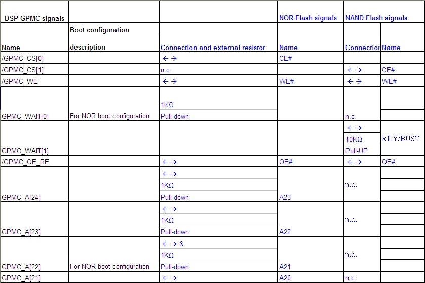
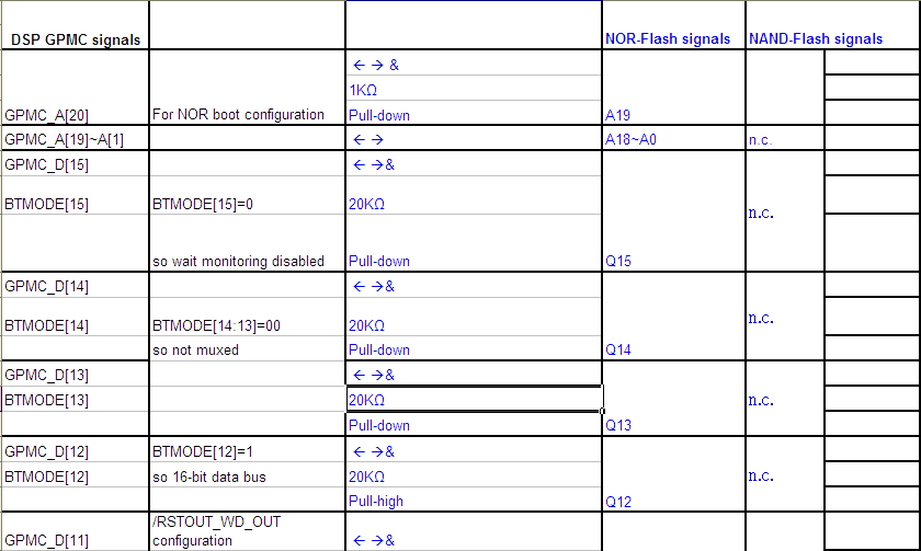
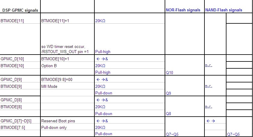
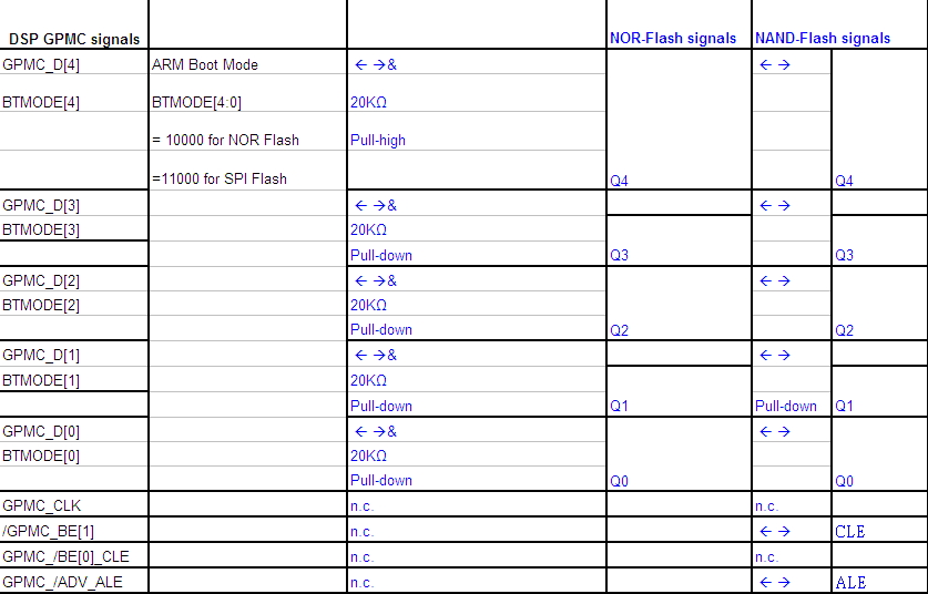
           If the product is a DVR, NOR Flash (16bit) is the code booting,

          and record images using NAND Flash (8bit), the circuit should be how to connect? Thank you

  • Hi Huang,
     
    They should both be connected to the GPMC interface. You can check tables 4-2 and 4-3 for the necessary signals. Please note that NOR Flash must be connected to GPMC_CS[0], the NAND can be connected to GPMC_CS[1...7], whichever is convenient. Also the RDY/BUSY signal from NAND can be either connected to GPMC_WAIT[1] if this pin is free, or totem-poled with the NOR WAIT signal to GPMC_WAIT[0], with an external pull-up resistor of 10kOhm in both cases.
     
    You can also use the EVM schematics as a reference (you will need both Base Board and Expansion I/O, since NOR is located on the second board). They can be downloaded from location:
     
     
    Best Regards
    Biser
  • Hi biser,

                    Thanks you reply.

                    Could  you tell me the refer to table 4-2 and 4-3 in what document?

                    Could you help to check the following table connection is correct? Thank you.

  • Hi Huang,

    A few notes from me:

    • NAND signal CLE should be connected to GPMC_BE[0]_CLE
    • GPMC_WAIT[0] should not be pulled down externally. This will cause the processor to wait forever.
    • Please read carefully "Advisory 2.1.33 XIP Boot: High-Order Address Handling (GPMC_A[27...13])" in the DM814X Errata. It can be found on the TI product page, and here is the link: http://www.ti.com/lit/er/sprz343a/sprz343a.pdf. You can refer to Page 28 of the EVM I/O Expansion board for reference to the workaround. I suppose this is the reason you placed all those 1kOhm external pull-downs on the high address lines.
    • Also don't forget to take into consideration the DM814X internal PU/PD resistors, which are enabled by default and can be reconfigured when the pinmux registers are set at U-boot time.

    Other than the above notes the connections look OK to me.

    Best Regards
    Biser
  • Hi Biser,

    1.Could you tell me the refer to table 4-2 and 4-3 in where document?

    2.XIP Boot: High-Order Address Handling (GPMC_A[27...13]):
        You proposal to use the EVM the I / O Expansion board for reference to the
        workaround.Not use to 1kOhm external pull-downs?

    3. Other ,this document, the page 1042 described
        GPMC_WAIT0 is configured for NOR (muxed and Non-muxed) with default settings
         in case we use as WAIT, else do a PULL DOWN
         and here is the link: http://www.ti.com/lit/ug/sprugz8b/sprugz8b.pdf
         Could you help to confirm this? thanks.

  • Hi Biser,

    1.Could you tell me the refer to table 4-2 and 4-3 in where document?

    2.XIP Boot: High-Order Address Handling (GPMC_A[27...13]): 
        You proposal to use the EVM the I / O Expansion board for reference to the 
        workaround.Not use to 1kOhm external pull-downs?

    3. Other ,this document, the page 1042 described
        GPMC_WAIT0 is configured for NOR (muxed and Non-muxed) with default settings 
         in case we use as WAIT, else do a PULL DOWN
         and here is the link: http://www.ti.com/lit/ug/sprugz8b/sprugz8b.pdf
         Could you help to confirm this? thanks.

  • Hi Biser,

    1.Could you tell me the refer to table 4-2 and 4-3 in where document?

    2.XIP Boot: High-Order Address Handling (GPMC_A[27...13]): 
        You proposal to use the EVM the I / O Expansion board for reference to the
     
        workaround.Not use to 1kOhm external pull-downs

    3. Other ,this document, the page 1042 described
        GPMC_WAIT0 is configured for NOR (muxed and Non-muxed) with
     default settings 
         in case we use as WAIT, else do a PULL DOWN
         and here is the link:
     http://www.ti.com/lit/ug/sprugz8b/sprugz8b.pdf
         Could you help to confirm this? thanks.

  • Hi Biser,

    1.Could you tell me the refer to table 4-2 and 4-3 in where document?

    2.XIP Boot: High-Order Address Handling (GPMC_A[27...13]): 
        You proposal to use the EVM the I / O Expansion board for reference to the 
        workaround.Not use to 1kOhm external pull-downs?

    3. Other ,this document, the page 1042 described
        GPMC_WAIT0 is configured for NOR (muxed and Non-muxed) with default settings 
         in case we use as WAIT, else do a PULL DOWN
         and here is the link: http://www.ti.com/lit/ug/sprugz8b/sprugz8b.pdf
         Could you help to confirm this? thanks.

  • Hi Huang,
     
    1. Tables 4-2 and 4-3 are on pages 155-157 in the DM814X datasheet (http://www.ti.com/lit/ds/symlink/tms320dm8148.pdf).
    2. Yes, this is the TI proposed workaround. I'm not sure, but 1kOhm pull-downs may be too strong and draw excess current when trying to drive these address lines high.
    3. This is correct for processor silicon version 2.0. Anyway, I don't think it will hurt if you provide an external pull-down. You can always remove it if it causes a problem with accessing NOR.
     
    Best Regards
    Biser
  • Hi Biser,

    Sorry, I'm a little confused, then GPMC_WAIT0 the follow connection the EVM EXP_IO_BOARD circuit design to the NOR Flash RY/BY and pull-up 10kohm or follow technical reference manual the will GPMC_WAIT0 pull-down? Could you help to confirm this? Thank you.

  • Hi Huang,
     
    First of all, does the NOR Flash (which you intend to use) have a RDY/BY signal? If it does, I think it will be wise to connect it to GPMC_WAIT0. RDY/BY may not be needed for reading from the NOR (read accesses are usually much faster than writes), but you may want to reprogram the Flash on-board, and then you will definitely need the RDY/BY signal. If you are not sure, I can suggest you provide place for a pull-up on this line next to the Flash, then a 0Ohm serial resistor, and after it place for a pull-down next to the processor. This will allow you to configure all possible connections without having to cut traces and patch components on the board.
     
    Best Regards
    Biser
  • Hi Biser,

    Thank you for the explanation.
    another design issue, MMC / SD Card and USB circuit design have any design document or suggest? Thank you

  • Hi Huang,
     
    The USB interface is on pages 27-28, and the SD/MMC interface is on page 16 of the EVM Base Board schematics: