This thread has been locked.

If you have a related question, please click the "Ask a related question" button in the top right corner. The newly created question will be automatically linked to this question.

Data transfer from C6678 to Virtex 6 FPGA over PCIe

Hi all,

I am trying to perform a data transfer between a C6678 EVM and a Virtex 6 ML605 EVM.

My hardware setup includes:

  1. The C6678 EVM connected to the AMC to PCIe adapter card
  2. Two PCIe connectors back-to-back connecting the PCIe lanes across the link and allowing the input of reference clocks (100MHz fed to the FPGA side)
  3. The Virtex 6 ML605 evaluation board.

My software setup includes:

  1. The LogiCORE IP Virtex-6 FPGA Integrated Block v1.7 for PCI Express loaded on the FPGA (programmed to boot form BPI flash at power on) (Created by following the ML605 PCIe x4 Gen2 Design Creation (PDF) reference design (link below))
  2. A CCS project for the DSP which began as the PCIe example project but has been greatly modified since.
I have successfully performed data transfers between two C6678 EVMs using DMA and MSI interrupts and performed throughput testing to match that described in the PCIe Use Case document (sprabk8).
I have solved problems establishing a link between the DSP and FPGA by including the 100 MHz reference clock to the FPGA (the DSP does not appear to require an external clock to maintain the link).
I can successfully access the FPGA's configuration registers (0x21802000 onwards) from the C6678 over the link after it is established. This has allowed my to ensure fields such as busMS and memSp are set on both sides.
I can however only read the FPGA's BAR addresses after remotely setting its BAR mask to 0xFFFF_FFFF. I have tried setting the DSP's outbound translation to this BAR value (appears as 0xFFF0_0000 between DSP and FPGA) but data transfer is still unsuccessful.
The PC seems to assign a different BAR address to that set in the Core Generator tool (0xFFF00000) which I assume is directly assigning the BAR address to the memory address.
I cannot access information about any inbound or outbound translation performed by the FPGA (or whether it even performs this) as this information is in the application space and not in the configuration space which, if I'm right, cannot be accessed across the link.

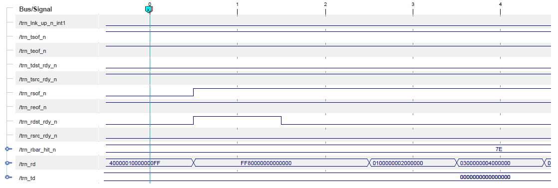
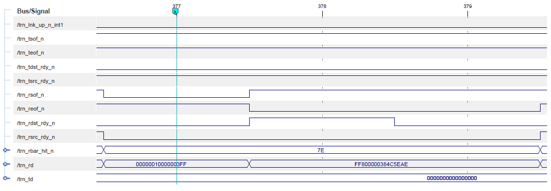
I know that the FPGA's core and accompanying application is operating correctly because I can connect it to a Windows XP PC and run a PCI Bus monitoring application (PCITree) that allows me to view the FPGA's configuration space, follow a BAR address through to the memory location it points to, and change the memory values successfully. I have wired the ML605 LEDs up to show the address line written to in memory (e.g. if writing to offset 0x0000_0005 the LEDs display 0000_0101 (binary 5)).

Therefore I know that the problem lies on the DSP side probably due to some wrong address somewhere or some other setup that the PC does automatically but my code is not doing. I can't however figure out where this problem lies.
When I try to take the FPGA and connect it to the DSP, I can connect fine but I cannot successfully write or read data (the LEDs do not light so I know the write is not happening like it did with the PC).

The following thread discusses the same problem, but the solution (removing accr checks) did not solve my problems:
I would welcome any of the contributors of that thread to post their working code so I can check for differences with my code (which may be trivial) to get data communication working.

Other background information that may be useful:
http://www.xilinx.com/support/documentation/ml605.htm
Virtex-6 FPGA Integrated Block for PCI Express
Reference Designs (free Xilinx website account creation required)

Many Thanks
Charles
  • I have since managed to insert ICON and ILA cores into the FPGA to observe signals associated with packet transfer. I have also now successfully seen evidence of a data packet transfer into the FPGA's user application corresponding to a memory write request. This began after I managed to configure the FPGA's BAR address to teh correct value (matching its memory request size):

    I also observe correct signal transitions and header field values for memory read requests however data is still not received by the DSP:

    I'm guessing by the lack of response that no one feels well enough informed to suggest a solution to my problem. I thought I'd post this anyway as it may be helpful to anyone in the future or someone might be able to help be me with advice on read requests instead.

    Thanks

    Charles

  • I have now successfully observed a read request completion with data, and been able to view the data in the DSP DDR using the CCS memory browser:

    However this was somewhat by accident as I experimented setting the data size I wanted to write and read to 65 (2x 32 DWORD + 1x 1 DWORD).

    As you can see, the 1 DWORD request is completed by the FPGA whereas the 32 DWORD requests go unfulfilled.
    I am using EDMA to perform both read and write. Write requests are executed fine with the data payload following the TLP header. 

    I have performed EDMA transfers between 2 C6678 in the past without this happening.

    Does anyone know how to solve this problem?
    Does the EDMA module need to be stalled before its next read request?
    or is it a problem with the FPGA not being able to reply to request greater than 1 DWORD?

    Thanks

    Charles

  • Hi Charles,

    I am trying to establish a communication between a DSP C6678 and a ML605 board too.

    I found the same problems than you did: I have needed to feed the ML605 with a 100MHz clock in order to set the link up.

    But I am having problems when transfering data. I am receiving in the trn_rd bus words that I didn't expected. When reading the PCIe standard specification, I have found that the data I receive is a kind of message request. Another thing I see is that trn_rsof_n and trn_reof_n don't activate, and I have seen that you had that problem too. Can you tell me how did you solve your problems with data transfering?

    Here is attached an image with the message received:

    Thank you very much in advance.

    Alberto.

  • Hello all,

    I know this is an old post but I am new to PCIe for C6678 and hope to get some help.

    First question to Charles: can you send me a picture of the connector?...did you have to manually connect TX to RX lines...I am trying to interface C6678 to SP605 FPGA and have the PCIE adaptor.

    I am using the PCIe example code under "C:\ti\pdk_C6678_1_1_2_6\packages\ti\drv\pcie\example\sample" and  "pcie_sample.c" to understand how to interface C6678 (RC)  to our SPARTAN6 FPGA (EP)  using the PCIe. In the example, they are using C6678 EVM and address translation is enabled. in my case, we instantiated a 4K DPRAM in the FPGA where we store data into and want to read the contents into the C6678 Multicore shared memory or DDR3 so all cores can access the same data. Any advice on how to change the code to achieve this specially the address translation part?. please if you have any code to share, my email is

    mqahwash@devry.edu

    Regards,

    Murad