Hello,
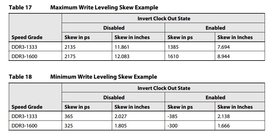
In the document "DDR3 Design Requirements for KeyStone Devices" SPRABI1A- April 2011, I have found in the paragraph ( 4.3.1.10 Write Leveling Limit Impact on Routing ) the constraint regarding the skew between the clock, addr ,command line and data , data strobe. In the table 16 and 17 there a minimum and maximum skew. The clock , addr and command line must be longer than data and data strobe. But it is right that addr , clock and command line must be longer almost 2 inch respect to the data and data strobe ?.
Now , my second release of layout in not yet finished.I have implemented about the same(skew < 0,8 inch) length between the addr, clock , command line and data and data , data strobe.