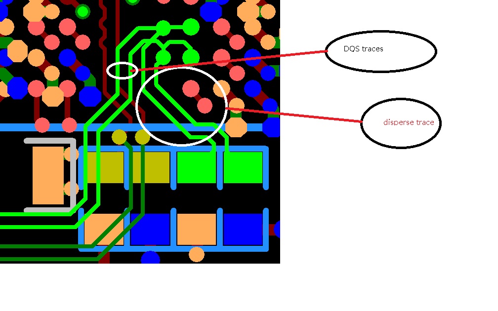
This thread has been locked.

If you have a related question, please click the "Ask a related question" button in the top right corner. The newly created question will be automatically linked to this question.

question about 8148 DDR3

Hi Sir,

I have a question about 8148 DDR3 controller, I want to use only one DDR3 controller ,how to do with the other controller?

from spec page 286,

Note that the 16-bit wide interface schematic is practically identical to the 32-bit interface (see Figure 8-54
and Figure 8-55); only the high-word DDR memories are removed and the unused DQS inputs are tied off.
The processor DDR[x]_DQS[2] and DDR[x]_DQS[3] pins should be pulled to the DDR supply via 1-kΩ
resistors. Similarly, the DDR[x]_DQS[2] and DDR[x]_DQS[3] pins should be pulled to ground via 1-kΩ
resistors.
When not using a DDR interface, the proper method of handling the unused pins is to tie off the
DDR[x]_DQS[n] pins to the corresponding DVDD_DDR[x] supply via a 1-kΩ resistor and pulling the
DDR[x]_DQS[n] pins to ground via a 1k-Ω resistor. This needs to be done for each byte not used.
Although these signals have internal pullups and pulldowns, external pullups and pulldowns provide
additional protection against external electrical noise causing activity on the signals.

just add pull up/down resistors to DQS pins is enough?

  • Hi Iverson,
     
    Yes, this is correct. Plus you should also check the line below yout quote: "Also, include the 50-Ω pulldown for DDR[x]_VTP. All other DDR interface pins can be left unconnected." Power supplies must also be connected. Datasheet section 4.4 deals with unused pins in general.
     
    Best Regards
    Biser

  • Hi  Biser,

    Thank you very much for your rapid reply!

    In my design, we used one DDR3 controller as our costdown product,and two DDR3 controllers(include CDDR0 and CDDR1) as High perphermace product,

    So I have to draw DDR3 memory and pull-up/down resisters in same design, this will make routing traces disperse, please see the trace below photo.

    Because the DQS and DQSn signals are very sensitive,I'm not sure this trace disperse may affect on Signal Integrity?

  • Hi Iverson,
     
    This makes it a little bit complicated indeed. I would suggest something like this: route DQS/DQSn traces from processor pad through pullup/pulldown resistor pad and then on to the memory chip. You can place these pullup/pulldown resistors whereever it' most convenient, no need to bunch them next to the processor where space is really tight. I'm even thinking that it will be better if they are on the far end of the lines, so that DQS/DQSn traces will not act as antennas when there is no memory attached.
     
    Another idea may be to break the DQS/DQSn traces by inserting 0Ohm resistors.
     
    Best Regards
    Biser