


TI Team,
I'm in the process of converting my L138 design into the AM1808. I have a few questions about clocking below:
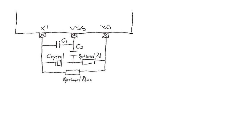
- Can the AM1808 24MHz clock (derived from the xtal oscillator) be buffered through pin T18?
- How do we configure the AM1808 registers to do this? I was unable to find Non-OS sample code that shows how to do this.
- Can the 24MHz oscillator be trimmed by using a small trim capacitor?
-David
