This thread has been locked.

If you have a related question, please click the "Ask a related question" button in the top right corner. The newly created question will be automatically linked to this question.

Loss in Image Quality when 24 or 16 bit image is displayed on LCD using DM 368

Dear TI

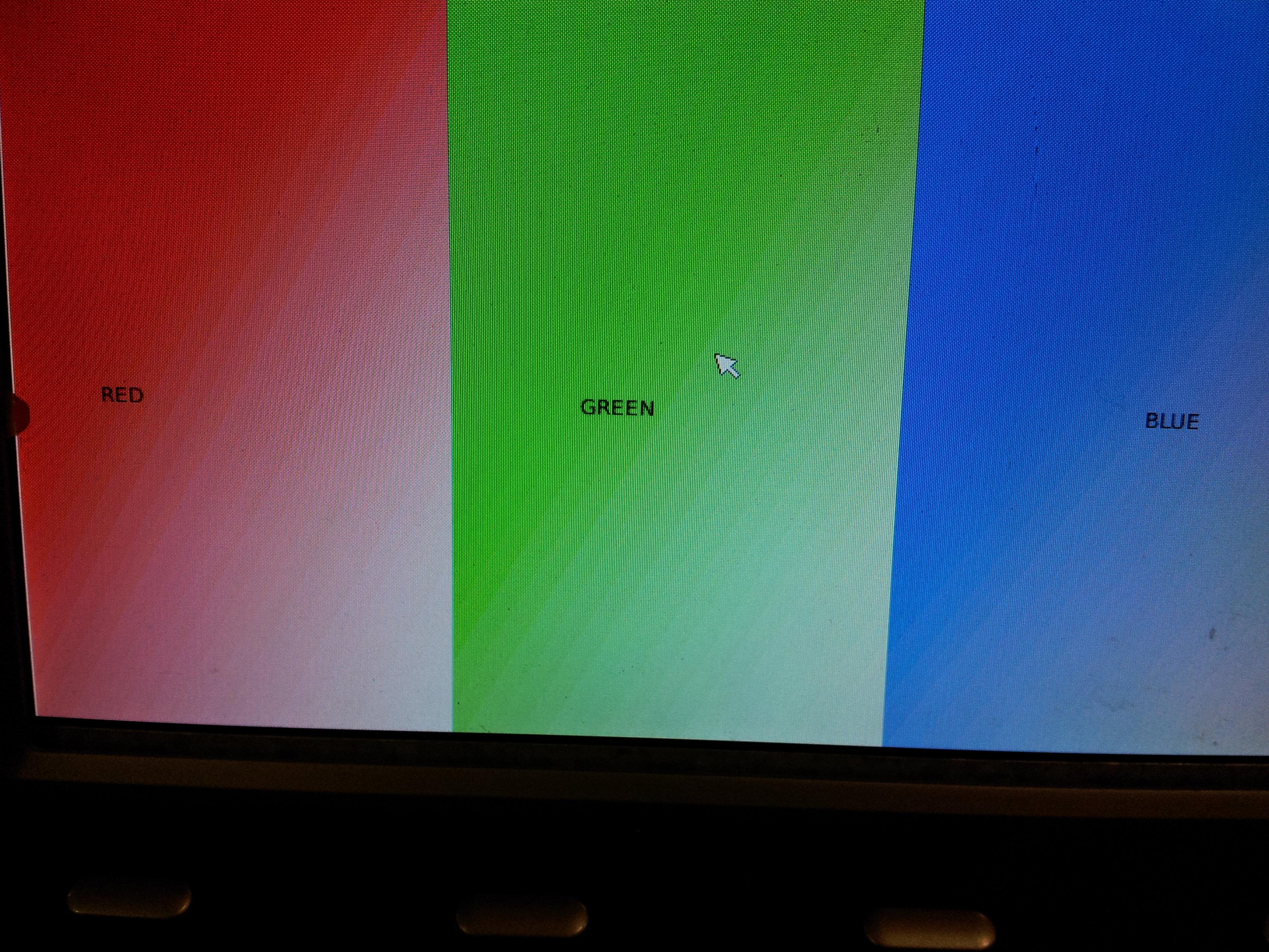
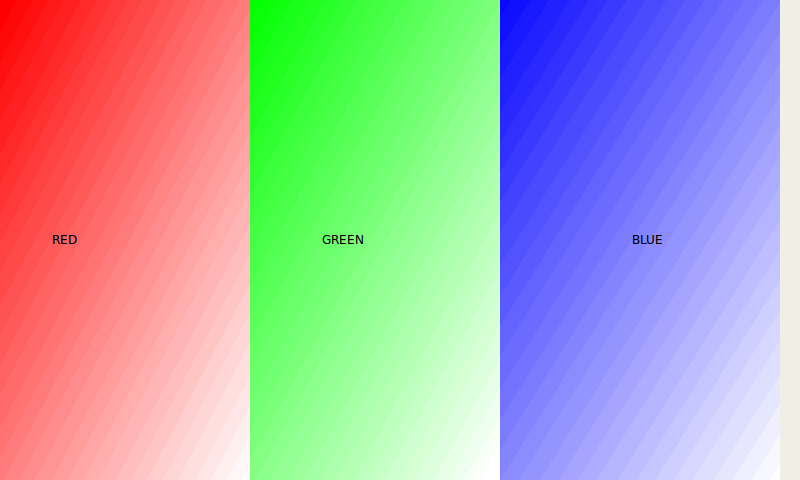
We are using DM 368 processor and a 24 bit PRGB interfaced LCD  (from Truly ) having  resolution of 800 * 480 ( size is 7 ''). We have an application which shows gradient of colors in Red, Green, Blue. This application was compiled for the PC and DM368. When we execute on PC Gradient looks very smooth there is no blocking effect (see PC_Image.BMP) but when we execute application for the DM368 we are getting blocking effect (see DM368_Image.BMP). It looks like it is showing application output in 16 bit colors.

We recompiled QT with 24 bit configuration only even then we are getting same result.

How to achieve 24 bit images of QT on LCD output of DM368.

Image Quality seen on PC

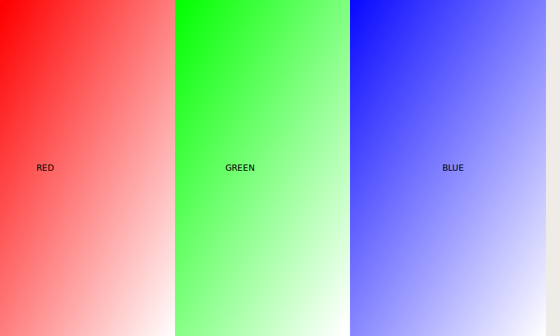
Image Quality When displayed on DM 368

Regards

pradeep

  • Pradeep,

    Interesting problem. Can you dump the VPBE->VENC registers and the System Control -> PINMUX registers and share?

    Also can you share the portion of the schematic where LCD is interfaced to?

  • Hi Renjith

             Pls find the schematic of our LCD interface, and the venc reg dump. Could you tell me which venc register we should look into ?

     regards

    pradeep

    1462.LCD _POWER.pdf

    0361.LCD INTERFACE.pdf

     VENC  Reg offset:   0   Value:     2011 
     VENC  Reg offset:   4   Value:     2000 
     VENC  Reg offset:   8   Value:        0 
     VENC  Reg offset:   c   Value:        f 
     VENC  Reg offset:  10   Value:       30 
     VENC  Reg offset:  14   Value:        3 
     VENC  Reg offset:  18   Value:      3ba 
     VENC  Reg offset:  1c   Value:       55 
     VENC  Reg offset:  20   Value:      320 
     VENC  Reg offset:  24   Value:      20b 
     VENC  Reg offset:  28   Value:       20 
     VENC  Reg offset:  2c   Value:      1e0 
     VENC  Reg offset:  30   Value:        0 
     VENC  Reg offset:  34   Value:        0 
     VENC  Reg offset:  38   Value:        0 
     VENC  Reg offset:  3c   Value:        0 
     VENC  Reg offset:  40   Value:     ff00 
     VENC  Reg offset:  44   Value:        0 
     VENC  Reg offset:  48   Value:        0 
     VENC  Reg offset:  4c   Value:        1 
     VENC  Reg offset:  50   Value:        0 
     VENC  Reg offset:  54   Value:        0 
     VENC  Reg offset:  58   Value:        0 
     VENC  Reg offset:  5c   Value:        0 
     VENC  Reg offset:  60   Value:        0 
     VENC  Reg offset:  64   Value:      800 
     VENC  Reg offset:  68   Value:        1 
     VENC  Reg offset:  6c   Value:        0 
     VENC  Reg offset:  70   Value:        0 
     VENC  Reg offset:  74   Value:        0 
     VENC  Reg offset:  78   Value:        0 
     VENC  Reg offset:  7c   Value:        0 
     VENC  Reg offset:  80   Value:        0 
     VENC  Reg offset:  84   Value:        0 
     VENC  Reg offset:  88   Value:        0 
     VENC  Reg offset:  8c   Value:        0 
     VENC  Reg offset:  90   Value:        0 
     VENC  Reg offset:  94   Value:        0 
     VENC  Reg offset:  98   Value:        0 
     VENC  Reg offset:  9c   Value:        0 
     VENC  Reg offset:  a0   Value:        0 
     VENC  Reg offset:  a4   Value:        0 
     VENC  Reg offset:  a8   Value:        0 
     VENC  Reg offset:  ac   Value:        0 
     VENC  Reg offset:  b0   Value:        0 
     VENC  Reg offset:  b4   Value:        0 
     VENC  Reg offset:  b8   Value:        0 
     VENC  Reg offset:  bc   Value:        0 
     VENC  Reg offset:  c0   Value:        0 
     VENC  Reg offset:  c4   Value:     7000 
     VENC  Reg offset:  c8   Value:        0 
     VENC  Reg offset:  cc   Value:      17a 
     VENC  Reg offset:  d0   Value:        0 
     VENC  Reg offset:  d4   Value:        0 
     VENC  Reg offset:  d8   Value:        0 
     VENC  Reg offset:  dc   Value:        0 
     VENC  Reg offset:  e0   Value:      100 
     VENC  Reg offset:  e4   Value:        0 
     VENC  Reg offset:  e8   Value:        0 
     VENC  Reg offset:  ec   Value:        0 
     VENC  Reg offset:  f0   Value:        0 
     VENC  Reg offset:  f4   Value:        0 
     VENC  Reg offset:  f8   Value:        0 
     VENC  Reg offset:  fc   Value:        0 
     VENC  Reg offset: 100   Value:      400 
     VENC  Reg offset: 104   Value:      57c 
     VENC  Reg offset: 108   Value:      159 
     VENC  Reg offset: 10c   Value:      2cb 
     VENC  Reg offset: 110   Value:      6ee 
     VENC  Reg offset: 114   Value:      400 
     VENC  Reg offset: 118   Value:      57c 
     VENC  Reg offset: 11c   Value:      159 
     VENC  Reg offset: 120   Value:      2cb 
     VENC  Reg offset: 124   Value:      6ee 
     VENC  Reg offset: 128   Value:        0 
     VENC  Reg offset: 12c   Value:        0 
     VENC  Reg offset: 130   Value:        1 
     VENC  Reg offset: 134   Value:        0 
     VENC  Reg offset: 138   Value:        0 
     VENC  Reg offset: 13c   Value:        0 
     VENC  Reg offset: 140   Value:       11 
     VENC  Reg offset: 144   Value:        0 
     VENC  Reg offset: 148   Value:        0 
     VENC  Reg offset: 14c   Value:        0 
     VENC  Reg offset: 150   Value:        0 
     VENC  Reg offset: 154   Value:        0 
     VENC  Reg offset: 158   Value:        0 
     VENC  Reg offset: 15c   Value:        0 
     VENC  Reg offset: 160   Value:        0 
     VENC  Reg offset: 164   Value:        0 
     VENC  Reg offset: 168   Value:        0 
     VENC  Reg offset: 16c   Value:        0 
     VENC  Reg offset: 170   Value:     d642 
     VENC  Reg offset: 174   Value:        0 


  • Pradeep,

    Can you share the panel datasheet and the PINMUX register settings?

  • Pradeep,

    One more thing. Can you share the schematic for the DM36x side of the LCD interface?

  • Renjith,

    I'm not sure of pin mux register settings. After going through the DM 368 document, i came to know that there are 2 pin mux registers pinmux 1 and 4. I've dumped the pin mux register 1  which dumped the value.:: INT_HDVICP_ENABLE === 0x001fc405 . If it is not correct, let me know how to dump pin mux register

    Psl find the schematic of LCD interfacing on DM 368

    regards

    pradeep

    7824.TFT1N1678-Ev1.0.pdf

    4478.LCD INTERFACE DM368 side .pdf

    2671.LCD INTERFACE DM368 side lower RGB bits .pdf

  • Pradeep,

    Instead of writing code to dump the value of PINMUX registers, you can use a utility called devmem2 which might be already available in your file system. You can use the tool and pass the physical address of the PINMUX registers, it will display the value on your console.

  • Renjith

     Thanks for the reply. As per your suggestion, i've dumped the pin mux 0 to 4 register values.

    pin mux 0: Read at address  0x01C40000 (0x40020000) val: 0x00FD0000

    pin mux 1: Read at address  0x01C40004 (0x40020004)  val: 0x00201555

    pin mux 2: Read at address  0x01C40008 (0x40020008) val: 0x00001800

    pin mux 3:Read at address  0x01C4000C (0x4002000c) val: 0x175AFFFF

    pin mux 4:Read at address  0x01C40010 (0x40020010) val: 0x55557CFF

    regards

    pradeep

  • Pradeep,

    Can you set PINMUX1 to 0x0028_5555 and check the output?

  • Renjith,

                  There is a little improvement in the picture but still it is not producing the same image as displayed on the PC. Pls find the reference picture. could tell me the problem why there is little improvement and why it is not producing the exact picture as displayed on PC ? Is there any problem in the schematic or interfacing to LCD ? As per my understanding, the loss in image quality may be due to the OSD module which merges and converts to yCbCr  (vid0,vid1, osd0,osd1)  first then to rgb 888 ? Here color conversion (from rgb 888/565 --> to yCbCr ----> rgb 888) is done and due to which there is loss in quality of image. A'm i right ?

    regards

    pradeep

  • Your understanding is correct. Finally everything is 16-bit. I'm still not really convinced whether this is the best possible with 16-bit or not. 

    Can we try to generate similar pattern with RGB565 and compare the output with this? 

    Also can you generate another Red pattern and with just four colors 0xFC0000 0xFD0000 0xFE0000 0xFF0000 where only four minor changes are there in the LSB. You can create four vertical bars with these colors and then see whether you are able to differentiate between the four red color bars? Similarly you can validate other bits of all colors. 

  • Renjith,

             When we tried to check if r0-r7, b0-b7, g0-g7 signals are coming from DM-368, we observed that r0,b0,g0 signals are low which means that the o/p from DM 368 is rgb 777 instead of rgb 888. I checked the pin mux 4 register setting, The Gio27,gio29,gio32 is enabled as per the pin mux 4 register settings. I do not why the o/p is not coming from the ro,b0,g0 pins ? do you have any idea on this ?

    pradeep

  • Are you sure that GIO27 28 and 32 are enabled or B0, B1, R0 is enabled in PINMUX4?

    Also can you check one simple thing. In the pattern that you are trying, can you set the R0, B0 and G0 bits to zero and try to view it in PC and see whether that matches with our display?

  • Renjith,

     Yes the r0,b0,g0 bits are enabled. the result is the when i disabled the gio 27,28 and 32 bits. The picture displayed on LCD matches with what is seen on pc when these bits are disabled. As i earlier said, the o/p of ro go bo pins are in LOW when seen in oscilloscope. i do not why there is no data on lower bit even though the gio pins of the pin mux 4 register are enabled

    For confirmation when i read the pinx mux 4 register its value is 55557CFF . As per the dm368 document, pin mux 4 register, bit 0-1 is Bo (gio 27) , bit 4-5 is g0 (gio 28), bit 10-11 is R0 (gio32)

    pradeep

  • Pradeep,

    The LSB bits may not be required to be set as 16-bit to 24-bit conversion is happening. 

    Pradeep Acharya said:

    Yes the r0,b0,g0 bits are enabled. the result is the when i disabled the gio 27,28 and 32 bits. The picture displayed on LCD matches with what is seen on pc when these bits are disabled. 

    Does that mean that your problem is solved?

  • Renjith

           the problem is not completely solved there is little bit improvement after correcting the pin mix 1 register.

    pradeep: "The picture displayed on LCD matches with what is seen on pc when these bits are disabled".

                     I think i've misunderstood what u were asking for ?  What i meant from the above statement is that the loss in the image quality seen when rgb_24 bit and rgb_16 bit color pattern displayed on LCD is  matches  when the image displayed on LCD is captured through an external camera and that captured image is checked on PC.

                   so if you are asking w . r. t  to the original image seen on PC vs what is displayed on LCD, there is an improvement after correcting the pin mux 1 register. The problem still exits and it is not completely solved. To know the reason for this when probed the r0-r7 signals we came to know that  R0,g0 and B0 bits are low and there is no signal generated through these pins.

                  The LCD panel is expecting  rgb 888 but currently the o/p from DM 368 is only rgb 777. I think the o/p from DM 368 should be rgb 888 and not rgn 777. There seems to be a problem from DM 368 side.

    pradeep

  • Renjith

                     In the schematics ro,bo,go was not connected that is why we were unable to see the signals . After connecting them, we are able to see signals on r0,b0,g0 pins. But still the image quality did not improve. It was same as before i,,e there is no impact on correcting the lower bits. This means that the o/p from DM 368 should be a problem ? Does it mean that the color conversion from 16 bit yuv to 24 bit rgb 888 is a problem in DM 368 ?.  Do you have any idea on the driver part which takes care of configuring the yuv to rgb conversion ? Should we suspect OSD module which merges the frames ?

    pradeep

  • Pradeep,

    We can't expect RGB888 from 16-bit YUV without data loss. But can we convert the same 24-bit image in PC to a 16-bit image and see whether it is same as the boards one?

    Then, can you write a small PC tool to just create 16 different images from the image file that you are using where you set bit 0, 1, 2, ..7 with 0 or 1. Compare the 16 different files and find out which one matches best to your LCD output.

    Assume that if there is any hardware line getting shorted or something wrong with the connections, we can figure out which bit is causing the trouble.