Hi,
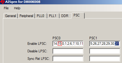
I followed http://processors.wiki.ti.com/index.php/Boot_Images_for_OMAP-L138 to boot DSP core from ARM. DSP LPSC (PSC0,#15) and PSC1.31 for shared_RAM have both been enabled (the explicit enabling of PSC1.31 in AISgen seems simply unnecessary and probably is redundant). Below are some basic settings:
|
AISgen version |
1.9, for D800K008 |
|
DSP's entry_point |
0x8000,0000
|
|
PSC |
PSC0.15 for DSP core PSC1.31 for 128K shared RAM |
|
ARM & DSP memory placement overlap |
No |
In ARM we have code for enabling the DSP core which was modified from .GEL file, but its internal steps is exactly the same as in the OMAPL138-DSP-LED-ARM example.
|
OMAPL138-DSP-LED-ARM |
/* Wake up the DSP */ CSL_FINST(psc0Regs->MDCTL[CSL_PSC_DSP], PSC_MDCTL_NEXT, ENABLE); CSL_FINST(psc0Regs->PTCMD, PSC_PTCMD_GO1, SET); while(CSL_FEXT(psc0Regs->PTSTAT, PSC_PTSTAT_GOSTAT1)==CSL_PSC_PTSTAT_GOSTAT1_IN_TRANSITION); CSL_FINST(psc0Regs->MDCTL[CSL_PSC_DSP], PSC_MDCTL_LRST, DEASSERT); |
|
My code modified from GEL |
//1. Set DSP boot address vector. SYSCONFIG->HOST1CFG = 0x80000000; //2. Disable core PSC0_LPSC_enableCore(1, LPSC_DSP); //3. De-assert local reset *(unsigned int*)(/*PSC0_MDCTL*/0x01C10A00+4*LPSC_DSP) |= 0x00000100; /* De-assert local reset for LPSC_DSP*/ |
This code:
- In very rare occasions I did see it wakes up the DSP successfully because I let the DSP do some work (generate a square on IO pins, blink LED, etc) and I can see these performed after board POR. Unfortunately, they happened only for a couple of times several days earlier and I was not able to reproduce this “correct” behavior now.
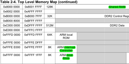
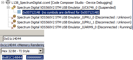
- For all times after the few exceptions in (1) later, I never had the luck to see DSP booting successfully from the snippets above again. In these cases, I connect to the DSP with XDS560V2 and see its PC at 0x007?????, by referring to “2.5 Memory Map Summary” of SPRS586C I see that this address is in the 1024K DSP L2 ROM. Reading of SYSCFG0.HOST1CFG show that “DSP boot address vector” is at one byte (=0x8000,0001) after the set 0x80000000 address and I have no idea if it should be exactly 0x80000000 and the 1 byte difference suggest some error. We also checked 128K shared RAM, memory inside DSP’s megamodule and DDR2 and found that all contents listed in the .map file has been correctly loaded.
I started to guess that the many unsuccessful attempts were due to fact that the DSP has not actually undergone a proper “reset” by the ARM core: it probably has been running upon startup and ignored the ARM’s action. If we look at either the OMAPL138-DSP-LED-ARM code or PSC0_LPSC_enableCore() that I adapted from .GEL, we would realize that they actually had no effect if the DSP’s LPSC is already enabled and the DSP is already running. The observation that the DSP’s PC address shown after emulator connection is still in its L2 ROM is also supportive of this speculation.
We therefore modified the code to:
- Disable the DSP core and assert its local reset (LRST) bit.
- Enable DSP core again and de-assert LRST bit.
|
Code that actually works and causes the DSP to boot: |
//1. Disable core first PSC0_LPSC_disableCore(1, LPSC_DSP); //2. Assert local reset *(unsigned int*)(/*PSC0_MDCTL*/0x01C10A00+4*LPSC_DSP) &= ~0x00000100;/*Assert local reset for LPSC_DSP*/
//1. Set DSP boot address vector. SYSCONFIG->HOST1CFG = 0x80000000; //2. Disable core PSC0_LPSC_enableCore(1, LPSC_DSP); //3. De-assert local reset *(unsigned int*)(/*PSC0_MDCTL*/0x01C10A00+4*LPSC_DSP) |= 0x00000100; /* De-assert local reset for LPSC_DSP*/
|
This code turned out to work and we could see DSP performing tasks we assigned; we could also communicate with DSP by CHIPSIG IPC interrupts and DSP responds correctly to those interrupts.
However a new problem arose: CHIPSIG interrupts to ARM would cause ARM core to jump to ARM ROM.
If we don’t enable CHIPSIG0 interrupt whose direction is to ARM only (see http://processors.wiki.ti.com/index.php/StarterWare_01.10.01.01_User_Guide), everything is fine and both ARM and the ARM-waken DSP could run and communicate; but once we have CHIPSIG0 interrupt on the ARM enabled:
|
Enable CHIPSIG0 interrupt |
IntRegister(SYS_INT_SYSCFG_CHIPINT0, isr_CHIPINT0); IntChannelSet(SYS_INT_SYSCFG_CHIPINT0,INT_CHANNEL_CHIPINT0); IntSystemStatusClear(SYS_INT_SYSCFG_CHIPINT0); IntSystemEnable(SYS_INT_SYSCFG_CHIPINT0);
… IntGlobalEnable(); |
Then the running of ARM would halt after it has wakened DSP with the above “Disable DSP->Assert reset->set HOST1CFG->Enable DSP->Deassert reset” snippet.
- One the DSP side everything works fine and DSP could perform tasks like blinking LED, generate GPIO wave, etc.
- All actions on ARM core stopped; if we also let the ARM manifest its own operation to the external world by also do actions like generating GPIO wave, these actions also stopped.
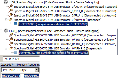
- If we connect to ARM with XDS560V2, we see ARM PC at 0xFFFF???? which is in ARM’s local ROM.
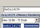
- We also see that at address 0x01c14174 CHIPSIG[0] signal has been asserted.
These observations suggest that CHIPSIG[0] interrupt is highly likely responsible for ARM’s sudden halting. We then tried to further narrow the search for the trouble maker by testing CHIPSIG[1], which also generates an interrupt to the ARM only:
|
Disable CHIPSIG0 interrupt
Enable CHIPSIG1 interrupt |
IntRegister(SYS_INT_SYSCFG_CHIPINT0, isr_CHIPINT0); IntChannelSet(SYS_INT_SYSCFG_CHIPINT0,INT_CHANNEL_CHIPINT0); IntSystemStatusClear(SYS_INT_SYSCFG_CHIPINT0); IntSystemDisable(SYS_INT_SYSCFG_CHIPINT0);
IntRegister(SYS_INT_SYSCFG_CHIPINT1, isr_CHIPINT1); IntChannelSet(SYS_INT_SYSCFG_CHIPINT1,INT_CHANNEL_CHIPINT1); IntSystemStatusClear(SYS_INT_SYSCFG_CHIPINT1); IntSystemEnable(SYS_INT_SYSCFG_CHIPINT1);
… IntGlobalEnable(); |
The result is:
- ARM could still wake up DSP and all subsequent running of both cores as well as inter-processor communication are normal.
- ARM is NEVER halted, and XDS560V2 connection show that ARM’s PC is at legal address such as 0xCxxxxxxx inside the DDR2, which is where we place the code.
CHIPSIG1 signal is NOT asserted; more importantly, CHIPSIG0 signal is also NOT asserted either. We found this surprising because the fact that we didn’t enable SYS_INT_SYSCFG_CHIPINT0 for ARM’s AINTC doesn’t prevent CHIPSIG0 bit from being set. However, why CHIPSIG0 would be set in the case when SYS_INT_SYSCFG_CHIPINT0 is enabled and when DSP wakes, is itself a mystery: we did no operation at all on the DSP side to interrupt ARM by writing to CHIPSIG0 bit, and we don’t know why it is asserted when DSP wakes when SYS_INT_SYSCFG_CHIPINT0 is also enabled in AINTC.
The problem related to CHIPSIG0/ SYS_INT_SYSCFG_CHIPINT0 does not occur only here: for waking up from DEEPSLEEP (described in http://e2e.ti.com/support/embedded/linux/f/354/p/211525/749623.aspx#749607), we found that
- For around one out of ten times the DEEPSLEEP wake could be unsuccessful when SYS_INT_SYSCFG_CHIPINT0 is enabled.
We are still working on this to see if in these cases ARM PC also points to local ROM and if CHIPSIG[0] is also automatically asserted without any such statement on both cores.
To summarize the content of this long post:
- Steps at http://processors.wiki.ti.com/index.php/Boot_Images_for_OMAP-L138 is not guaranteed to wake DSP. We found that ARM might need to disable DSP, assert local reset first before do the steps listed by the wiki article. This probably suggest that after AISgen boot DSP core is already running even before ARM enables it , though with PC point at DSP L2 ROM location.
- SYS_INT_SYSCFG_CHIPINT0 cannot be enabled on the ARM side: if it is enabled, after waking up DSP CHIPSIG[0] bit will get set without any statement DSP executes to set it. ARM will jump to its local ROM address.
- If we don’t enable SYS_INT_SYSCFG_CHIPINT0 and enable SYS_INT_SYSCFG_CHIPINT1 only, we will not have the problem in (2), and in fact NO bit in CHPGSIG[0-4] will get set.
- The mysterious CHIPSIG[0] set in (2) seems also related to ARM’s occasional halting after waking up from DEEPSLEEP mode, and we are still investigating it. In addition we have also checked L138 errata SPRZ301H’s “Advisory 2.1.5 A Single CHIPINTn Interrupt Event Will Register Multiple Times in the DSP Event Combiner Module (ECM)” and “Advisory 2.1.12 A Single CHIPINTn Interrupt Event Can Register Multiple Times in the AINTC”, but these two notes cannot explain CHIPSIG[0]’s “unsolicited” behavior here.
Also regarding our “Disable DSP->Assert reset->set HOST1CFG->Enable DSP->Deassert reset” approach I still have an unresolved doubt:
- Without the leading “Disable DSP->Assert reset”, the latter enabling/reset operation is not effective, and our screenshot above has shown that the DSP’s PC incorrectly points to DSP L2 ROM. What is the content there? If there are legal instructions inside DSP L2 ROM, Would the seeming aimless and random execution of instructions corrupt the memory region, either in the 128K shared RAM or DDR2, that the ARM is going to use?
We use our own board rather than a standard EVM; if the documented problems here can be reproduced on standard EVMs, I guess it might perhaps deserve some attention from the chip designer? Is it another undiscovered issue that needs to be added to the errata?
Paul