This thread has been locked.

If you have a related question, please click the "Ask a related question" button in the top right corner. The newly created question will be automatically linked to this question.

PCIe link up problems in FPGA connecting to DSP

Hello, I get PCIe link up problems in FPGA connecting to DSP. The C6678 DSP works as RC and the V6 FPGA works as EP. But I hardly get link up in both sides.

On our custom board, I have achieved the DMA communication between two V6 FPGAs. And the FPGA communicates with DSP based on PCIe protocol as well. My partner use the example provided by TI. When we first try it, both sides got link up well. Then, sometimes DSP prints “Link is up” while FPGA’s trn_lnk_n is not stable and sometimes both sides can’t get link up.

We change the x2 gen2 link to x1 gen1 link. The trn_lnk_n becomes stable. In the first try, trn_lnk_n is asserted. But after that trn_lnk_n is always high. We also try to make FPGA as RC and DSP as EP. And the results are same as before.

According to Xilinx AR#34151, I find the 8b/10b RX errors happened. After PIPERX#ELECIDLEGT goes low, the PIPERX#STATUSGT doesn't stay 000b stably. And PIPERXVALIDGT is unstable as well. The signal trn_lnk_n doesn’t assert although the pl_ltssm_state hops well.

An external PLL provides the clocks to FPGA and DSP. We have compared the quality of it to the clock which supports the communication between two FPGAs. They are comparable. So we pay attention to the Training Sequences. We compare the FPGA Rx’s TS with FPGA-FPGA’s case and do some changes. But that doesn’t impact the unstability of PIPERX#STATUSG and PIPERXVALIDGT, and trn_lnk_n doesn’t assert.

What causes these problems? Is it the bad signal integrity or the mismatch configuration in link training between C6678 DSP and V6 FPGA?

sincerely,

  • Xing,

    When you see the link up issue happens, could you check the LTSSM_STATE field of DEBUG0 (0x21801728) register in C6678 PCIe module to see which LTSSM state it is please? Please refer to the section A.1 in PCIe user guide for the LTSSM state decoding. 

    And are you trying the C6678 PCIe LLD example on C6678 device please? By default, the LLD example configures the C6678 PCIe as x1 Gen1 (

    gen2.dirSpd = 0x0; //not change to Gen2 speed after link is initialized at Gen1 speed
    gen2.lnEn = 1; //1 lane enabled

    I am not sure which configuration is supported by the FPGA, but during the link training, both sides will communicate the operation mode to each other and the link will be established with the maximum configuration supported by both sides (i.e. x1 Gen1 if using the default setup in LLD).

    If you are able to see the link up sometimes, it may indicate the issue is due to the signal integrity, such as the reference clock and TX/RX connectivity. Please check the Hardware Design Guide (SPRABI2) document for the PCIe connection details. And please also check the document on the FPGA side to see if any special requirement needed.

  • first thank you for your reply ,steven

    i have been using the c6678 PCIe LLD example in the 6678pdk for this test.

    first  

    when the link up didin't happen ,the LTSSM state were mostly varying  between 0x2 and 0x3.

    In the first couple days when we began to test this ,there was a little probability that we can finish the link training and get link up (the ltssm state was surely 0x11). However , using the same code ,we can hardly succeed now.

    I'm checking the register now and will reply later.

    but i'm eager to know if it was about the signal integrity , how can i prove it and how to sovle this ? is there anything i can do except to redesign the PCB?

    thank you 

    sincerely!

  • the gen2 register for lane num and dirspd

    we have test both option(change the configuration on the FPGA side as well ) ,it seems that no difference happened.

  • Xing,

    It looks like the PCIe is stuck at Poll.active and Poll.compliance states. It might be the presence of a passive test load (e.g. a register) which force the lanes to enter Polling.Compliance.

    And some customers observed the similar issue due to the bad PCIe reference clock that the PLL could not be locked (either FPGA side of DSP side).

    Please take a look at the following post to see if it helps.

    http://e2e.ti.com/support/dsp/c6000_multi-core_dsps/f/639/p/218446/770888.aspx#770888

  • dear Steven Ji

    thank you again first.

    I've seen this post . and I think this must be a hardware problem.  

    But how do i fix the pll problem? there is a "LB" filed in the PCIE_SERDES_CFGPLL register,will it help if i change this part from 0h to 2h?(medium bandwidth to low bandwidth), i'll  check this later

    an the for the " It might be the presence of a passive test load (e.g. a register) which force the lanes to enter Polling.Compliance", i don't quite understand, e.g a register ? can you explain it a little more?

  • and for my board , i have two v6 fpga and two 6678 dsp. we have succeed in the pcie link between two fpga, so i don't think this is the problem in fpga part

    and if it w

    xing wang said:

    Hello, I get PCIe link up problems in FPGA connecting to DSP. The C6678 DSP works as RC and the V6 FPGA works as EP. But I hardly get link up in both sides.

    On our custom board, I have achieved the DMA communication between two V6 FPGAs. And the FPGA communicates with DSP based on PCIe protocol as well. My partner use the example provided by TI. When we first try it, both sides got link up well. Then, sometimes DSP prints “Link is up” while FPGA’s trn_lnk_n is not stable and sometimes both sides can’t get link up.

    We change the x2 gen2 link to x1 gen1 link. The trn_lnk_n becomes stable. In the first try, trn_lnk_n is asserted. But after that trn_lnk_n is always high. We also try to make FPGA as RC and DSP as EP. And the results are same as before.

    According to Xilinx AR#34151, I find the 8b/10b RX errors happened. After PIPERX#ELECIDLEGT goes low, the PIPERX#STATUSGT doesn't stay 000b stably. And PIPERXVALIDGT is unstable as well. The signal trn_lnk_n doesn’t assert although the pl_ltssm_state hops well.

    An external PLL provides the clocks to FPGA and DSP. We have compared the quality of it to the clock which supports the communication between two FPGAs. They are comparable. So we pay attention to the Training Sequences. We compare the FPGA Rx’s TS with FPGA-FPGA’s case and do some changes. But that doesn’t impact the unstability of PIPERX#STATUSG and PIPERXVALIDGT, and trn_lnk_n doesn’t assert.

    What causes these problems? Is it the bad signal integrity or the mismatch configuration in link training between C6678 DSP and V6 FPGA?

    sincerely,

    ere the pll that could not be locked on dsp side.  how can it pass the 

    /* Wait until the PCIe SERDES PLL locks */
    while (!lock)
    {
    CSL_BootCfgGetPCIEPLLLock(&lock);
    }

    part ?

    or  am i having a fault understanding of this part?

  • dear Steven

    for today's further test , we found the following phenomenon:

    1. In the PCIE_SERDES_STS register(SPRUGS6C p32):

    it's value is 0x309 after power reset.  which means the LOSDTCT1, LOSDTCT0,SYNC1 is 1.

    after our configuration, it will become 0x109(x2)or 0x101(x1),  this is very weird ,because  for the successful link up ,it will be 0x1.

    the LOSDTCT(lost of signal detect) and sync(Symbol alignment) should be 0.  I don't get much information about these fields and don't understand well, I hope you or someone can explain this.

    2. In the PL_LINK_CTRL register

    there is a DLL_EN field(enable link initializtion) which should be 1as default, howerver  mine is 0 , and i must assert it myself. for this ,it seems that ,the odd for successful link up can be bigger.

    3. when i set the pcie as 2x , after link up ,however , in the fpga side ,we just got lane1 without any data(link training sequence )

    what do you think these phenomenon suggest?

    thank you !


  • Xing,

    1.Each receive lane supports loss of signal (also known as electrical idle) detection, configured via the RX_LOS bits of SERDES_CFG0/1 registers.  

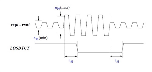
    When enabled, the differential signal amplitude of RXp and RXn is monitored. Depending on whether it is below or above the threshold levels, the LOSDTCT bit of PCIE_SERDES_STS register is asserted high or low respectively, as shown in the figure below. The threshold levels are described by e30 in the figure, which is normally min=75mVdfpp, max=125mVdfpp.

    When the differential signal amplitude crosses the threshold, LOSDTCT will change state asynchronously within 50ns (t33). 

    When LOSDTCT is asserted high, clock recovery will stop, and the state is retained.

    2. DLL_EN is for the DLL Link Enable. If DLL_EN=0, the core does not transmit Flow Control DLLPs and does not establish a link. By default it should be 1. I am not sure why you have to assert it yourself. But it seems to be required for a successful link up.

    3. I am not sure how the FPGA is configured in your design. Does the FPGA supports 1 lane or 2 lanes? And are you connecting the Lane 0 of DSP to Lane 0 of FPGA and Lane 1 of DSP to Lane 1 of FPGA please? Lane 0 is the master lane in DSP and it should be connected no matter for x1 mode or x2 mode.

    I think the lost of signal may be due to some hardware issue on your board that the receive signal could not meet the threshold requirement. And when LOSDTCT is 1, the clock recovery is stopped, which may affect the link up.

    So I am wondering if you could improve the signal integrity on your board. Or you could try to disable the lost signal detection by setting RX_LOS=0 in both SERDES_CFG0 and SERDES_CFG1 registers to see if the link up could be done successfully. 

    And DLL_EN should be 1 as you observed and you could also try to re-train the link by toggling the LTSSM_EN bit in CMD_STATUS register, i.e. if the link is not up, you could de-assert the LTSSM_EN bit and then assert LTSSM_EN bit again to re-train the link. Hope those could help.

  • dear Steven

    I think it is Christmas holiday these days, Thank you very much for your help!  Happy New Year in advance.

    I'll check what you've supposed.

    And for what I've not described clear:

    In FPGA,we create a 2-lane core. We do connect the Lane 0 of DSP to Lane 0 of FPGA and Lane 1 of DSP to Lane 1 of FPGA.And in further test we found sometimes FPGA detects 1 lane and sometimes it detects 2 lanes.In FPGA,the user guide states"When the 2-lane core is connected to a device that implements only 1 lane, the 2-lane core trains and operates as a 1-lane device using lane 0".It means that the 2-lane core in FPGA supports 1 lane connecting when only 1 lane is detected.

    And  I still have a question, You said " if you could improve the signal integrity on your board",Does it mean that I have to redisign it? We've been puzzeld for a long time,because it only have 4 wire between the dsp and FPGA.  What can we do more?

     best regards!