This thread has been locked.

If you have a related question, please click the "Ask a related question" button in the top right corner. The newly created question will be automatically linked to this question.

Is it no problem that it does not exist pulldown resister on CKE and ODT pin between AM335x and DDR2 connection?

Guru 10570 points

Hello.

I am gonna use DDR2 as memory of AM335x system.
On datasheet Figure5-38(sprs717e P155), it specifies that the CKE pin and ODT pin are connected between AM335x and DDR2 immediately.
Is it no problem that it does not exist pulldown resister?

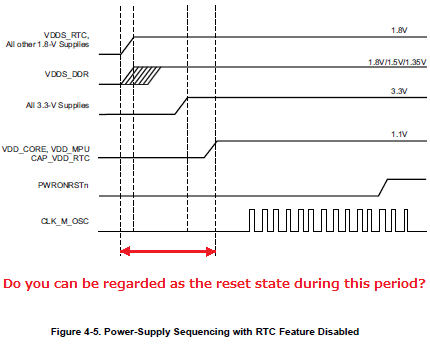
Since the datasheet specifies the "BALL RESET STATE", I understand that CKE and ODT pin hold Low state after AM335x power up.
But, I am taking care about before completion of AM335x power up.
Because, AM335x needs the power up sequence: 1.8V --> 3.3V --> 1.1V

My question is:
  Are the CKE and ODT held on Low state during power up?
  Does it not needed pulldown resister?

Best regards, RY

  • Hi RY,
     
    Both CKE and ODT are pulled low during reset (by internal pulldown), and driven actively low at reset release (by I/O buffer). There is no need, nor is it recommended  to place any additional external pulldown resistors on these signals for DDR2 configuration.
  • Biser-san.

    Thank you very much for helping me.
    Sorry, may I confirm this additionally?

    Our design holds Low state on PWRONRSTn pin during power up sequence. (which is powered up: 1.8V --> 3.3V --> 1.1V)

    During this power up time, can I think that it is hold Low state on CKE and ODT by internal pulldown resistor?

    Best regards, RY

  • Yes, Check Table 2-7 in the AM335X datasheet (columns Ball Reset State and Ball Reset Rel. State).
  • Biser-san.

    I appreciate your strong support.
    We checked the table 2-7(Ball Reset State and Ball Reset Rel. State).

    But, our customer have focused on whether "the Ball Reset State" is applied during power up.
    During this period each power is not turned on in the normal operating range.

    Sorry to trouble you.
    Could you check again about below question?

    Best regards, RY 

  • RY,
     
    I don't understand what's the problem here. What do you expect to happen during power-up, when neither processor, or EMIF or DDR are initialised?
  • Biser-san,

    Because it is requirement of JEDEC standard for DDR, I have to take care about whether the ODT and CKE are able to maintain the L level during this period.
    Can I think it is satisfied? (Are both ODT and CKE "L level" on the Figure above?)

    Best regards, RY

  • Hi RY,
     
    Of course it is satisfied. There are thousands of AM335X boards already manufactured with DDR2 memory. If you use a TI recommended PMIC and follow the datsheet design guidelines everything will be OK.
     
    As a sideline you could provide place for a 10kOhm pulldown on the CKE line, which is useful in order to enable memory self-refresh when the processor enters low-power modes.
  • Biser-san,

    Biser Gatchev-XID said:
    Of course it is satisfied. There are thousands of AM335X boards already manufactured with DDR2 memory. If you use a TI recommended PMIC and follow the datsheet design guidelines everything will be OK.

     
    Thank you very much!

    Biser Gatchev-XID said:
    As a sideline you could provide place for a 10kOhm pulldown on the CKE line, which is useful in order to enable memory self-refresh when the processor enters low-power modes.

    I'm sorry. I can not understand above meaning.
    Is it mean that the CKE becomes Hi-Z when the AM335x enters low-power modes?
    Can you tell me what you are concerning about?

    Best regards, RY

  • I discussed your concern with our expert today.  He has agreed to reply to your post with a detailed explanation how the AM335x is compliant to this JDEC requirement during power-up.

    I could answer your question well enough to make you feel comfortable this is not an issue, but I know his answer would provide more details and be more complete.

    Please give him a day or two to clear his queue and answer your question.

    Regards,
    Paul

  • Paul-san,

    Thank you so much for your support.
    We would like to wait answer from your expert.

    Best regards, RY

  • RY,

    I reviewed your concern. I'm presuming you are following all the power up sequencing requirements that are listed in the data sheet.

    Case 1: If you are ramping VDDS and VDDS_DDR supplies together.

    As the PWRONRSTn is held low and when VDDS and VDDS_DDR supplies are ramped to a certain threshold voltage (about 1V), an internal weak pull down pulls the CKE and ODT terminals low. This will guarantee that the CKE and ODT terminals will stay low even before the entire supply power up sequencing is completed.

    Case 2: If you are ramping VDDS supply first and VDDS_DDR follows VDDS.

    As the PWRONRSTn is held low and VDDS is fully ramped or reaches a certain threshold voltage (about 1V) AND VDDS_DDR voltage reaches a certain threshold voltage (about 1V), an internal weak pull down resistor pulls the CKE and ODT terminals low. This will guarantee that the CKE and ODT terminals will stay low even before the entire supply power up sequencing is completed.

    Given this, we should meet the DDR specification to maintain CKE and ODT low. DDR2 memories required CKE to be low to tri-state the data bus and avoid any contention with the Processor also driving data bus. This situation will never occur on AM335x due to the fact that AM335x never drives the data bus during initialization but just enables a weak pull and protect the inputs from floating.

    Please let us know if you have any more queries on this.

  • Sivak-san,
    Thank you very much for your advise.
    May I have another question?

    Can I think that also all other pins except ODT and CKE hold "BALL RESET STATE" during power on sequence?
    Off course, we would like to follow all the power up sequencing.
    Best regards, RY 

  • Hi RY,
    Please see in answer above:
     
    sivak said:
    ................AM335x never drives the data bus during initialization but just enables a weak pull and protect the inputs from floating.
  • RY

    Just to confirm again - the pad state during power on is not just for CKE and ODT but for all the pins. Basically, after VDDS supply reaches a certain threshold voltage and the power supply for the corresponding IO terminal reaches a certain threshold voltage, AM335x pad state would be defined as noted in the data sheet when held under Reset. This is true before the entire power supply sequencing is complete.

    Please let us know if you have any further queries to close this issue.

    Regards, Siva

  • Siva-san,

    Thank you for your support.
    It is very helpful for us.
    May I have final confirmation on this?

    From your answer:  

    sivak said:

    AM335x pad state would be defined as noted in the data sheet when held under Reset. This is true before the entire power supply sequencing is complete.

     - Can I think that it would be defined regardless of the voltage VDDSHV6(1.8V / 3.3V)?

    And once more question:
    Since the "BALL RESET REL. STATE" is "Z" on DDR_D0 pin[M3 on ZCZ pkg],
    I think it may be float between an access and next access.
    On GPMC case, it is prevented by Bus keeper circuit.
    It is described in TRM 7.1.3.3.9.10 (spruh73g: P278)

    Can I think there are some circuits to prevent it on DDR?
    Because, the externel PU/PD is no needed on DDR_Dx (sprs717e: Figure5-38).

    Best regards, RY

  • Siva-san,

    I am sorry to trouble you.
    It is last day that is completed schematics of our customer today.
    If you have trivial information, would you tell me?

    Best regards, RY

  • RY

    AM335x pad state defined in the data sheet is valid when VDDSHVx is set as 1.8V or 3.3V. Basically, VDDS and VDDSHVx have to reach the required threshold voltage for the pull values to take effect.

    >> Can I think there are some circuits to prevent it on DDR?

    There are weak internal pull up/down resistors available on the DDR IO terminals if required. Details on this are covered in TRM section 9.3.89/9.3.90

    Please let me know if you have any other queries.

    Regards, Siva

  • Siva-san,

    Thank you so much for your answer.
    I read the section 9.3.89/9.3.90 on TRM.
    There is a description of "Weak keepser".

    What is the "Weak keeper"? (How does it to operate?)

    Best regards, RY

  • Siva-san,

    Sorry to trouble you...
    I think that the "Weak keeper" is the same of bus keeper on GPMC.
    It keeps last state on DDR bus. Is that right?

    Best regards, RY

  • RY

    Weak Keeper will hold the previous state of the IO terminal when the output driver is disabled.

    Regards, Siva

  • Siva-san,

    Thank you very much for your answer.

    > AM335x pad state would be defined as noted in the data sheet when held under Reset.
    > This is true before the entire power supply sequencing is complete.

    Think about the case that VDDSHV6 is configured as 3.3V. (I emphasize that VDDSHV6 is the power supply voltage of PWRONRSTn)
    During power on sequence, the period which 1.8V is ON and 3.3V is OFF, can it be considered as all the pins powered from 1.8V are reset state defined in the datasheet? (Of course PORz is L level.)

    I guess there is some kind of mechanism on PWRONRSTn.
    It is because the power of PWRONRSTn (that is 3.3V) is not supplied to the VDDSHV6 yet in the period which I described above.
    Why can you know that PWRONRSTn is L level?

    Best regards, RY