Hello.
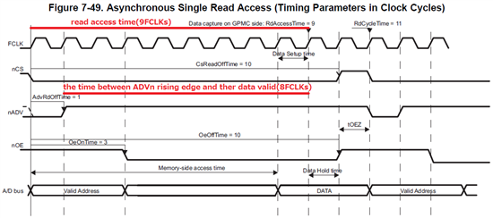
I have refered TRM 7.1.4.1.4(spruh73g: P358).
It describes that:
First, on the memory side, the external memory makes the data available
to the output bus. This is the memory-side read access time defined in Table 7-49:
the number of clock cycles between the address capture (ADVn rising edge) and
the data valid on the output bus.
But, it seem that the read access time(9FCLKs) does not equal the time between ADVn rising edge and ther data valid(8FCLKs) in table 7-49.
Which description is correct?
Best regards, RY


