This thread has been locked.

If you have a related question, please click the "Ask a related question" button in the top right corner. The newly created question will be automatically linked to this question.

The connection of VDDS_RTC on TMDSSK3358

Guru 16800 points

Hi,

I'm using a TMDSSK3358 board and checking the schematic of it.
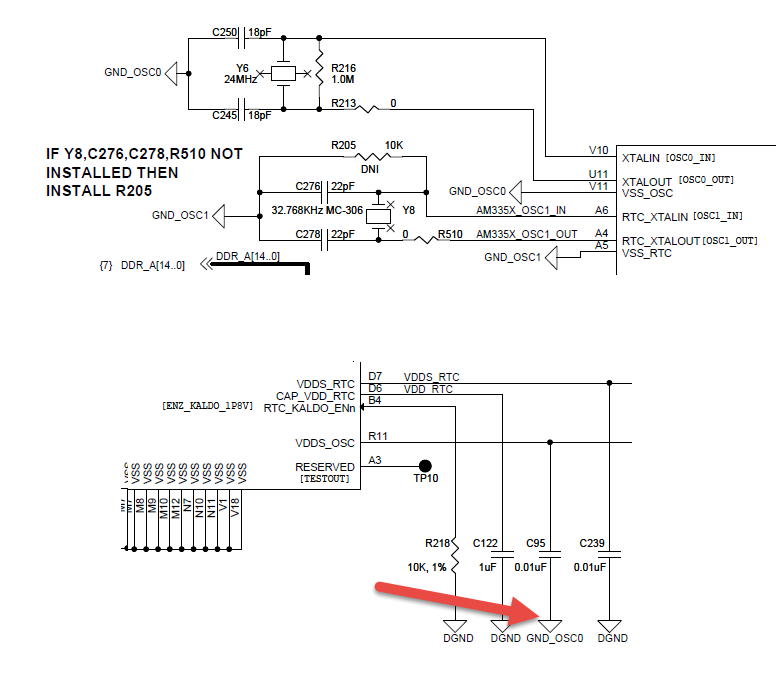
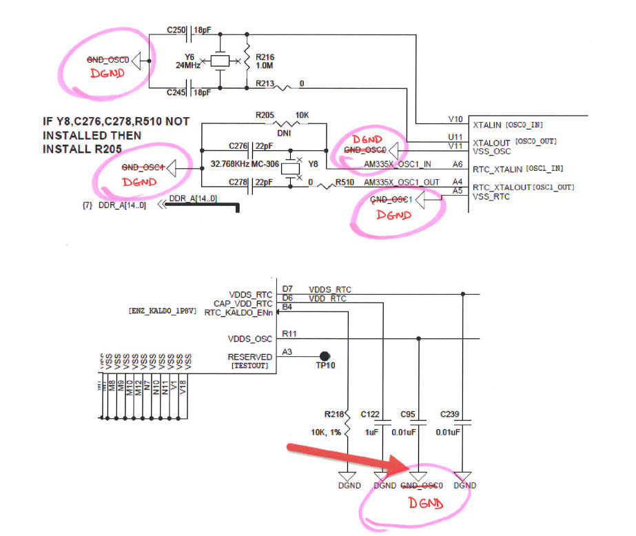
VDDS_OSC is connected to VSS_OSC (GND_OSC0) through a bypass capacitor, but VDDS_RTC is connected to DGND through a bypass capacitor.

Should VDDS_RTC be connected to VSS_RTC (GND_OSC1) through a bypass capacitor?
And, is the ground of VRTC VSS_RTC?

Thanks

Nomoto

  • Hi Nomoto,
     
    VDDS_RTC is the supply voltage for the whole RTC domain, not only for the RTC oscillator, therefore the decoupling capacitor is connected to common GND.
    VSS_RTC is the ground for the RTC oscillator only.
     
    VDDS_OSC is the supply voltage only for the main oscillator, therefore the decoupling capacitor is connected to VSS_OSC.
     
  • The current revision of the AM335x Data Sheet has the following note attached to the VSS_OSC and VSS_RTC terminals.

    This terminal provides a Kelvin ground reference for the external crystal components. External crystal component grounds should only be connected to this terminal and should not be connected to the PCB ground plane.

    I plan to modify this note in the next revision of the data sheet to help clarify the purpose of the VSS_OSC and VSS_RTC terminals.

    The new notes will be:

    The VSS_OSC terminal provides a Kelvin ground reference for the external crystal components. If a crystal circuit is connected to the XTALIN/XTALOUT terminals, the crystal circuit component grounds should only be connected to the VSS_OSC terminal and should not be connected to the PCB ground plane.  If an external LVCMOS clock source is connected to the XTALIN terminal, the VSS_OSC terminal should be connected to VSS.

    The VSS_RTC terminal provides a Kelvin ground reference for the external crystal components. If a crystal circuit is connected to the RTC_XTALIN/RTC_XTALOUT terminals, the crystal circuit component grounds should only be connected to the VSS_RTC terminal and should not be connected to the PCB ground plane.  If an external LVCMOS clock source is connected to the RTC_XTALIN terminal, the VSS_RTC terminal should be connected to VSS.

    The VSS_OSC and VSS_RTC terminals should not be used for decoupling capacitors.  Please refer to the Clock Specifications section of the AM335x Data Sheet for information related to the expected use cases for these terminals.

    Regards,
    Paul

  • A selected SMD crystal package has two connections for the crystal & two connections to shield the package case.

    Should the GND_OSC Kelvin connection be loaded with the crystals' metal case?

    Or are the only crystal components being referred to C1 & C2?

    Thanks,

    Russ

  • Yes.  If the SMD crystal package has ground terminals, they should also be connected to the kelvin ground.

    Regards,
    Paul 

  • Peaves;

    I question your statement about VDDS_OSC. What should a designer use for a reference for the bypass cap on VDDS_OSC? Your answer was not clear or maybe not just to me. I get the VSS_OSC & VSS_RTC and the crystal circuits but not how I should decouple the VDDS_OSC pin.


    Thanks in advance, Jeff

  • This is an old thread and our recommendation for connecting the VSS_OSC terminal has changed.  See Advisory 1.0.30 in the AM335x Silicon Errata.

    The OSC0 1.8 volt positive power terminal is VDDS_OSC and the ground terminal is VSS.  The VSS_OSC terminal is a Kelvin ground returning from the oscillator circuit.

    Previously we recommended the VSS_OSC terminal only be connected to the ground connections of the crystal components.  However, our current recommendation is to connect the ground connections of the crystal components and the VSS_OSC terminal to same digital ground as all the other VSS terminals.

    Regards,
    Paul

  • Paul;

    Thanks for the response. Now my question is what could result from having it connected per the original suggested connections? We are in production with over 2k produced so far. I am not seeing any issues but want to understand what may be lurking... I have inserted a snippet of my current connections. Thanks in advance for your help.


    Regards, Jeff

  • The VSS_OSC terminal has a higher impedance connection to the internal ground of OSC0 that the VSS terminal, so the decoupling capacitor is not as effective as it could be if it were connected VSS rather than VSS_OSC.

    The TI EVM has the same mistake and we have not had any reports of this causing a problem.  However, the EVM is normally used in a lab and may not be exposed to the same environmental conditions (like temperature variations, external electrical noise, and etc) as a production product.

    Based on my experience, I would be much more concerned with the issue described in Advisory 1.0.30.

    Regards,
    Paul 

  • Paul;

    Thank you for the prompt responses. We have about 1200 units installed all over the country and are not seeing any issues. We had one unit have a clock that was slow but changing out the AM335x fixed that. Just for clarity are you saying I should make the following changes?

    If not, can you adjust it so that I can make a running change to my board?

    Thanks again in advance for your help/time.

    Regards, Jeff

  • Yes, the ground connection of C95 should have always been connected to DGND.

    Connecting the crystal component grounds and the respective VSS_RTC or VSS_OSC terminal to DGND has proven to improve noise immunity on several systems.

    This change should only improve the crystal circuit noise immunity, but I would still recommend validating this change in your product before applying it to production.

    Connecting the crystal component grounds and the respective VSS_RTC or VSS_OSC terminal to DGND through a zero ohm resistor would give you the option to have it either way.

    Regards,
    Paul


  • Paul;


    Thank you. Do you know if TI will ever get the EVM schematics caught up so us developers do not continue to implement wrong designs? Very frustrating as I had my design verified by a TI FAE and they said it was correct.

    I will correct my design and test it before going to production. Thanks again for your responses!

    Jeff