This thread has been locked.

If you have a related question, please click the "Ask a related question" button in the top right corner. The newly created question will be automatically linked to this question.

PCIe : How to setup x2 link width and 5 Gbps link speed ?

Hi,

I am using C6678 dsp and PCIe interface for communicating with a FPGA. DSP is root complex and FPGA is endpoint.

I want to increase my PCIe link width from x1 to x2. What I am going to do is :

  1. MAX_LINK_WIDTH bitfield of LINK_CAP register will be set to 2.

  2. LNK_MODE bitfield of PL_LINK_CTRL register will be set to 3.

  3. LN_EN bitfield of PL_GEN2 register will be set to 2.

also I want to increase link speed from 2.5 Gbps to 5 Gbps. What I am going to do is :

  1. TGT_SPEED bitfield of LINK_CTRL2 register will be set to 2.

  2. MAX_LINK_SPEED  bitfield of LINK_CAP register will be set to 2.

Are these adjustments at DSP side enough for my requirements ? Are there any other register settings that I must be aware of ?

Regards,

koray.

  • Koray,

    I think your list is sufficient for x2 lane setup.

    For GEN2 link rate (5Gbps), you may want to check the note in section 2.3.3 of PCIe user guide that "Set the DIR_SPD bit to 1 in the PL_GEN2 register during the initialization can switch the PCIe link speed mode from Gen1 (2.5Gbps) to Gen2 (5.0Gbps)."

    Although you set 1 to "DIR_SPD" field, it will not show being set after the initialization. Instead, you can check the "LINK_STAT_CTRL" register that "NEGOTIATED_LINK_WD" field will show the link width (lane number, 0x1=x1 lane, 0x2=x2 lane) and "LINK_SPEED" field will show the link rate (0x1=GEN1, 2.5Gbps; 0x2=GEN2, 5.0Gbps).

    And please make sure the FPGA will support x2 lane and GEN2 speed as well. 

  • Hi Steven,

    I did the modifications written above and it seems working.

    After link up , I checked  the LINK_STAT_CTRL register and saw both x2 link width and 5 Gbps link speed are asserted in the related bitfields.

    But there is another point that I didn't understand: I did a basic data rate measurement that I just measured the time elapsed for a fixed size of transfer for both before and after the modifications. And saw that the data rate is just 2 times faster than the previous PCIe configuration. I was expecting it will be 4 times faster (2 times for link width, 2 times for link speed).

    Am I right about expecting the data rate to be 4 times faster ? or Am I doing something wrong about the data rate measurement ?

    regards,

    koray.

  • Koray,

    You are using EDMA for the PCIe data transfer, is it correct?

    I am wondering if you tried the delta measurement for the throughput testing. For example,  you could do data transfer twice (with different data size) in each scenario (x1 Gen1 vs x2 Gen2). Then the throughput could be (data_size_larger - data_size_smaller)/ (time_elapsed_larger - time_elapsed_smaller) for each scenario. You could compare the throughput measured in this way, which removes the constant latency involved in timing stamp capture. The latency may affect the throughput if the data size is relatively small and if you only capture the throughput once.

    I am not sure if you will see exactly 4 times improvement. But if both DSP and FPGA are setup correctly, I assume the data rate of x2 Gen2 should be more than 2 times better than x1 Gen1. And you could compare with PCIe throughput mentioned in the Throughput Performance User Guide which is in the case of x2 Gen2.

  • Hi Steven,

    You are correct, I am using EDMA for the PCIe data transfer. I am transfering 64 KB data which is not a small sized data transfer I guess. Anyway, I did your delta measurement but there had not been significant difference at data rate compared to my previous measurement.

    The data rate I find is 94MB with 5 Gbps and x2 lane configuration which is very slow according to the PCIe throughput results at the Throughput Performance guide(It should be 806 MBps). Now I am looking for why my throughput is so slow.

    1. How I am doing data rate measurement : I am using Timestamp module. When I am about to start EDMA transfer, I get initial time with 'Timestamp_get32()' and I do the last time measurement via the same function in the EDMA Callback Interrupt Handler. Then I simply subtract and divide : (Last time - initial time)/freq_nanosec to find the time elapsed. The result is approximately 683000 ns. And from this number I find the data rate is 94 MB.  Is there anything wrong with this measurement ?
       
    2. The PARAM set of EDMA channel I am using is as follows:

      paramSet.srcBIdx = 128;
      paramSet.destBIdx = 128;
      paramSet.srcCIdx = 128*512;
      paramSet.destCIdx = 12*512;


      paramSet.aCnt = 128;
      paramSet.bCnt = 512;
      paramSet.cCnt = 1;

      paramSet.bCntReload = 512;

      paramSet.linkAddr = 0xFFFFu;

      paramSet.opt = 0x0u;

      paramSet.opt &= 0xFFFFFFFCu;

      paramSet.opt |= ((tcc << OPT_TCC_SHIFT) & OPT_TCC_MASK);

      paramSet.opt |= (1 << OPT_TCINTEN_SHIFT);

      /* AB Sync Transfer Mode */
      paramSet.opt |= (1 << OPT_SYNCDIM_SHIFT);

      /* Static mode is ON*/
      paramSet.opt |= (1 << OPT_STATIC_SHIFT);

      I am setting A count to 128 in order to use EDMA in burst mode. 

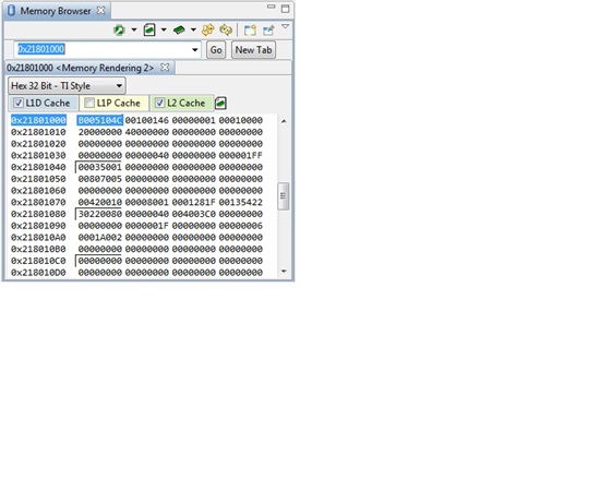
    3. The local register settings of PCIe interface after link up is attached. Please find it. This is for 5Gbps and x2 lane scenario. You also can see the other register settings that I use. 
    4. I recognised that LINK_CAP register is read-only. So the register settings that I was trying to do related with this register is meaningless. Right ?
       
    5. Another weird observation : After setting FPGA core to 5 Gbps and x2 lane setting, whether the negotiated link speed and negotiated link width is 2.5 Gbps or x1 lane based on the DSP preferences; the data rate is all same.
      I am meaning that FPGA core supports 5 gbps and x2 lane. But I am limiting DSP at 2.5 Gbps or x1 lane setting by means of LİNK_CTRL and GEN2 register settings. And I see that negotiated link speed is 2.5 Gbps and negotiated link width is x1 as expected. But data rate is does not change, it is always 94 MBps independent of the negotiated link speed and link width as long as FPGA supports 5 Gb and x2 lane. Do you have any idea on this ?

      Regards,
      koray. 


  • Koray,

    1. I think the Timestamp module in BIOS is using the Time Stamp Counter (TSC) in CorePac as well, but it may be worth trying to read the TSCL/TSCH registers directly in your testing. The CSL may have some details of the usage, such as "CSL_tscEnable (void)" and "CSL_Uint64 CSL_tscRead (void). 

    Please also make sure the device PLL has been configured correctly to certain frequency (such as 1GHz). The TSC will increase one for every CPU clock, so TSC counting 1 is 1ns for 1GHz device, but 10ns for 100MHz.

    Another thing is I am not sure if the EDMA callback ISR will introduce some overhead when you capture the stop time stamp. Are you able to keep polling the EDMA IPR register for the channel completion event and capture the time stamp right after that please? 

    We may want to remove all the overhead introduced by the software if you want to verify the PCIe link rate only.

    2. The EDMA setup seems OK, although the STATIC field seems to be set 0 instead of 1 for DMA channels, mentioned in the EDMA user guide (Table 2-3 OPT Field Descriptions).

    And please note the EDMA DBS in C6657 is only 64bytes. Please refer to the C6657 data manual (Table 7-31 EDMA3 Transfer Controller Configuration).

    You can still keep ACNT to be 128B. The EDMA with DBS=64B will just breakout the data into two transactions for PCIe. So you can refer to the throughput in 64B case.

    3. The register seems to indicate it is x2 GEN2 mode.
    4. The description in the LINK_CAP bit fields says some bits are internal writable which means the local device could change the value internally. But the external device could not modify the register over PCIe link since it is read-only by external device. Basically you can keep the default values in this register (indicating the maximum rate and lanes supported) and you can change the rate and lane number in PL_GEN2 register.
    5. I am not sure about the FPGA setup. We may want to complete the actions in #1 first to see if we could get any reasonable throughput.
    If possible, you can connect two C6657 together and try to see the throughput results in different scenarios.
  • Hi Steven,

    1. I tried your suggestions but the result is same:

      I see that PLL is set to 1 Ghz in gel file console output. So this means 1 cycle is 1 ns.
      I used TSCL register instead of 'Timestamp_get32()' .
      I kept polling EDMA IPR register instead of assigning an interrupt handler.

      In all cases, the measurement results are similar. Around 683000. And it means 683000 ns for 64KB data. 
    2. I used 64 as A count and increased B count twice. Result is same.
    3. I don't have an possibility of connecting two DSPs via PCIe interface.

    regards,
    Koray.


  • Koray,

    I may start looking at the FPGA side as well. Do you know what the maximum payload size the FPGA support for PCIe please?

    In C6657 PCIe, we support up to 128B but EDMA limits it to 64B. If FPGA supports less than 64B, then there will be much more overhead in each packet and the effective throughput will be lower even it says Gen2 X2 on both DSP and FPGA sides.


  • Hi Steven,

    We figured out that FPGA PCIe clock is just 125 MHz. So that's why our PCIe data rate is limited to 94 MBps.

    In these circumstances, It seems meaningles to use 5Gbps link speed as long as FPGA is driven at 125 Mhz PCIe clock.

    Thanks for your help,

    koray.


  • Hi Steven,

    Is it possible to increase the throughput of PCIe by using 64-bit memory adressing in our circumstances?
    FPGA's internal data width seems to work with 64-bit adressing.

    Also is there any other way to increase throughput of PCIe in our case that you can suggest ?

    Regards,
    Koray.


  • Koray,

    The 64-bit memory addressing is just the virtual PCIe address over the PCIe link. The payload size in each PCIe packet (TLP) will still be the same for either 32-bit addressing or 64-bit addressing.

    I am a little confused about the FPGA PCIe clock. Do you mean the 125MHz is the PCIe reference clock input to FPGA or something else?

    Normally the PCIe reference clock could be low jitter clock with frequency as low as 100MHz but the SerDes data rate will be Gen1 (2.5bps) or Gen2 (5.0bps) per lane after the SerDes PLL.

    So as long as the SerDes data rate from FPGA matches Gen1 or Gen2, the throughput should be in a reasonable range. 

    But normally we'd better use the same reference clock for both peers over the PCIe link. The C66x EVM is using 100MHz as PCIe reference clock on board. 

  • Hi Steven,

    At FPGA side, our PCIe reference clock is 100 Mhz but the clock that we are using at PCIe user logic is 125 Mhz.
    (Before, our user logic clock was 62.5Mhz and the data rate was half of current rate)
    So even if the Serdes can work at 2.5 Gbps or 5Gbps, FPGA user logic works at 125 Mhz. There is continuous data stream that flows from FPGA to DSP and FPGA can reply read requests of DSP just at 125 Mhz. And this is the bottleneck in our case.

    Now, we will try to drive FPGA PCIe user logic at 250 Mhz. Hope it works!

    Is there anything that you can suggest ?

    koray.


  • Koray,

    I see. You are talking about the interface clock, the one used by parallel-to-serial converter, right?

    Then it seems to be the hardware limitation. I do not see other way to workaround it unless we increase the clock frequency on FPGA side.