This thread has been locked.

If you have a related question, please click the "Ask a related question" button in the top right corner. The newly created question will be automatically linked to this question.

PLL2 and DDR3 Initialization over PCIe

We have a C6655 configured as an endpoint  that we are trying to initialize its PLL2 and DDR3 over the PCIe interface by the root port using a similar process found in the evm gel scripts so that we can download its application code to DDR3 and run.

I am having problems with configuring the PLL2 and DDR3 registers.  I have tried to "unlock" the KICK0 and KICK1 registers accordingly but it appears that my PCIe writes to the C6655 over PCIe are not working.  I know I have set my address translation tables correctly as the read operation for these registers appear to be correct and returning reasonable values.

1:  Can the KICK registers be unlocked by the root port over PCIe ?

2: Can the PLL2 and DDR3 registers be configured over PCIe or only by the Local C6655 Core 0 ?

3: Do we need to configure PLL1 and other things in order to setup the PLL2 and DDR3 ?   (we think the default PLL1 would work for us)

Can you please answer the above questions and provide som further suggestions into this problem.

Thanks


  • SID814,

    Did you set the MST_PRIV bit to 1 in 3.1.14 Transaction Priority Register (PRIORITY) before doing this?

    16 MST_PRIV Master transaction mode. PCIe transaction needs to be in supervisor mode to access the device registers.

    1 = PCIe transaction is in supervisor mode.

    Regards, Eric

  • Eric,

    We have set the MST_PRIV bit over PCIe  and have verified that via our emulator that it is set on the C6655.

    We however still cannot set the KICK and device registers accordingly.

    1: Is it allowed to set the PLL2 and device registers over PCIe by the root port ?

    2: Do you have any other suggestions to try ?

    Thanks


  • PLL2 registers are the device registers and should be able to set via PCIE link. We didn't try this but we did some other device registers (:

    1) myiowrite32(((ioread32(pReg1 + PRIORITY/4))|0x00010000), pReg + PRIORITY/4);   

    2) /* Unlock KICK0, KICK1 */
     myIowrite32(KICK0_UNLOCK, pReg2 + KICK0/4); ==============>pReg2 points to 0x2620000
     myIowrite32(KICK1_UNLOCK, pReg2 + KICK1/4);

    #define DSP_BOOT_ADDR(n)             (0x040 + (4 * (n)))
    #define IPCGR(n)                     (0x240 + (4 * (n)))

    3) myIowrite32(addr, pReg2 + DSP_BOOT_ADDR(core)/4); ======> we try to write an address to run from there after DSP core out of reset
     

    This works for us. Are you able to try if you can write an arbitary value to DSP_BOOT_ADDR and verify by emulator? This is to understand if you can't access device register at all or only can't access PLL2 registers?

    Regards, Eric

  • Eric-

    My apologies in advance for bumping an old thread, but this one comes up for searches such as "DDR3 registers over PCIe".

    Is it possible to *only read* DDR3 controller registers over PCIe ?  We have tried with PCIe supervisor mode transactions, and so far no luck.  Thanks.

    -Jeff
    Signalogic

  • Jeff,

    There are multiple issues here.  All bus masters, including PCIe, have the ability to write and read memory-mapped registers required for programming the PLLs and DDR3 controller and PHY.  There may be PCIe mapping issues that need to be resolved but that is no different than any other memory accesses.

    The original thread was concerned with configuring these devices over PCIe.  This has to be done as a multi-step process.  Programming sequences for the PLLs and the DDR3 controller and PHY have specific sequence constraints and required delays between some of the accesses.  This cannot be guaranteed through this type of interface.  Therefore, the solution is to load a small program into L2 memory from the PCIe and to then execute this program.  This program can initialize the PLLs and DDR3 controller and PHY same as if the program was loaded from a bootable memory device local to the DSP.

    Tom

  • Hi Tom-

    We're able t read DDR3 PLL registers (for example 0x02620330), but we cannot read:

      DDR3 SDCFG register at 0x21000008

      PCIe PID register at 0x21800000

    (result is 0xffffffff).  We use the same BAR1 setup in all 3 cases.


    -Jeff


  • All-

    It turns out that for external PCIe access to DDR3 MMRs to work, these steps must be done in c66x code:

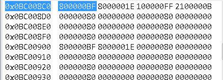
      -write to mem location 0x0bc008c8 a value of 0x100000ff
      -write to mem location 0x0bc008cc a value of 0x2100000b

    This sets up MPAX mapping for PCIe master access (with a privilege ID 11), and from that point the host can access 0x21000xxx (up to 512 bytes) and get correct results.  In c66x code, if you read at 0x0bc008c0, you should see the following:


    Note that these locations are shown as "Reserved" in the c6678 data sheet, so suggest to be ultra-careful to write only the required two (2) values. 

    -Jeff
    Signalogic