This thread has been locked.

If you have a related question, please click the "Ask a related question" button in the top right corner. The newly created question will be automatically linked to this question.

Help required to decide Multiple DSP booting (6457)...

Hey,

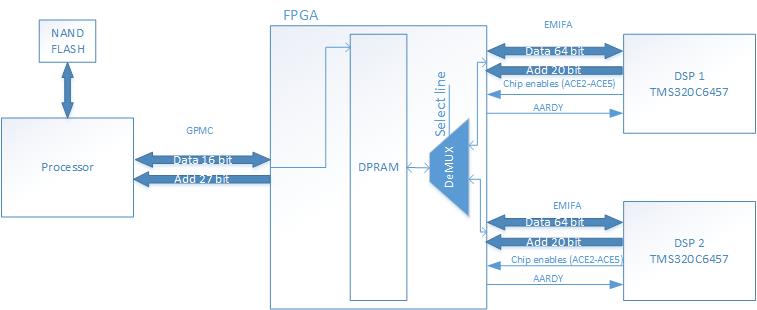
I have a design where 4 DSPs (TMS3206457) are interfaced with ALTERA FPGA through EMIFA interface. I have designed t he board such that the default boot mode selection is EMIF. The power is given simultaneously to all the 4 DSPs. The design does not contain dedicated FLASH device for each DSP, hence  the DSP gets its code frm the DPRAM on the FPGA. I am planning to keep a single DPRAM in the FPGA, and by using a MUX inside the FPGA to select the DSP EMIFA data and address lines to select each DSPs. Now, when i am loading the code for DSP1, will the other DSPs be waiting for the data so tat it automatically takes the data when i change the selection line to 2nd DSP or should i control the DSP using the POR??

  • Akshay,

    When each DSP is released from its RESETn signal, each DSP will start trying to read and execute from its EMIF bus. There is nothing inherent to the DSP that will cause it to wait for another DSP to complete its bootload process first.

    What does the "MUX inside the FPGA to select the DSP EMIFA data and address lines to select each DSP" actually do? The four DSPs will all be driving their EMIF address and control lines at the same time, so you have not explained anything that can be done to select one or another DSP.

    You will need to have some arbitration logic to hold off any DSP that you do not want to have access to the DPRAM at any particular time. Please refer to the EMIF User's Guide for more information on signals to use for bus arbitration.

    Regards,
    RandyP

  • HI Randy P,

     Firstly, i will use a De-multiplexer to choose the data and address pins inside the FPGA. After the 1st DSP reads the program, i'l use the select line to choose the nxt DSP. As i tried to understand in depth, i discovered that when EMIF boot mode is selected, the DSP waits at CE3 which has a base address at 0xB0000000. Does this affect the design of my DPRAM?? How does my chip select act for booting through EMIF?? Since EMIF boot is a 8bit asynchronous, can i use the ARDY pin to indicate the DSP to wait till my boot code is ready?? Im sorry if my question are too basic, I have worked on FPGAs but not on DSPs!

  • Akshay,

    Please draw a picture of what you are trying to do. Show the 4 DSPs and the FPGA and the major logic and signal busses.

    You are talking about a very complex system that you could be designing different ways. From my side, I do not know anything more to say besides what I have said above, with what I understand of your system at this point.

    Regards,
    RandyP

  • The above block diagram gives a simplified approach of what im trying to design.  I have A NAND Flash which contains the program of Processor , FPGA and the DSPs. IN the block diagram above im just representing 2 DSPs so that the design is simpler to understand, but in actual i have four DSPs. The power to Processor, FPGA and DSP is given in parallel, then the Processor is programmed, it programs the FPGA, then it writes the DSP1's program into the DPRAM in FPGA, now the DeMUX selects DSP1  interface to interact with the DPRAM. Now my queries are,

    1. During the time taken to program the Processor, the FPGA and writing the DSP1's program into the DPRAM in FPGA, during this time, what will my DSP1 and DSP2 be doing?

    2. Will it be waiting at the corresponding location n take the data moment the data is available or can we use the AARDY pin to indicate that the DATA is ready to be read.

    3.the datasheet says that it will be waiting at CE3 at 0xB0000000 location, should i consider this when im designing my DPRAM? If yes, den how?

    Thank you.

  • Akshay,

    The picture helps a lot.

    1. If the DSP is held in reset, it will not be doing anything until RESET is released. Once RESET is released, the DSP will start reading from its boot location. You can either use RESET or AARDY to hold off each of the DSPs. Please check the datasheet and the respective User Guides to find out if there are maximum durations for either. There is also a HOLD mechanism available on the EMIF, but that is probably not needed in this case.

    2. The EMIF User Guide explains the details of the EMIF's operation. Once out of reset, the DSP will start reading from its boot location regardless of whether the data is ready or not. You can use the AARDY signal to hold that off until you are ready for the read operation to be completed. As I mentioned above, please check the datasheet and the EMIF User Guide to see if there are any restrictions on this use of AARDY.

    For debug and testing purposes, I recommend you have a way to set the boot mode to the No Boot mode so you can debug in spite of any problems that might come up with the FPGA during initial debug.

    Have you considered replacing the four C6457s with one C6674 or one C6670? You may have your reasons for this design, but it is a thought worth mentioning.

    Regards,
    RandyP

  • Hi Randy,

    Thanks for the reply. It answers 80% of my queries. About the AARDY pin, are u sure i can use it during the boot through EMIF? As i have seen in the timing diagrams, i have never seen the use of AARDY signal for the same. And yes i have considered the use of quadcore / multicore processor, that would be the next version.

    Regards

    Akshay

  • Akshay,

    You can use AARDY as described in the datasheet and EMIF User Guide to extend any read or write access until AARDY goes to the Ready state.

    My concern is whether there is a maximum duration that AARDY can be held off before the EMIF cycle will be aborted. I doubt this is the case, but the only way to find out is if there is a statement to that fact in the datasheet or EMIF User Guide. If there is no statement to this effect, then you are okay.

    Regards,
    RandyP