This thread has been locked.

If you have a related question, please click the "Ask a related question" button in the top right corner. The newly created question will be automatically linked to this question.

DM8167 DVO2 output PAL Setting Question

Hi:

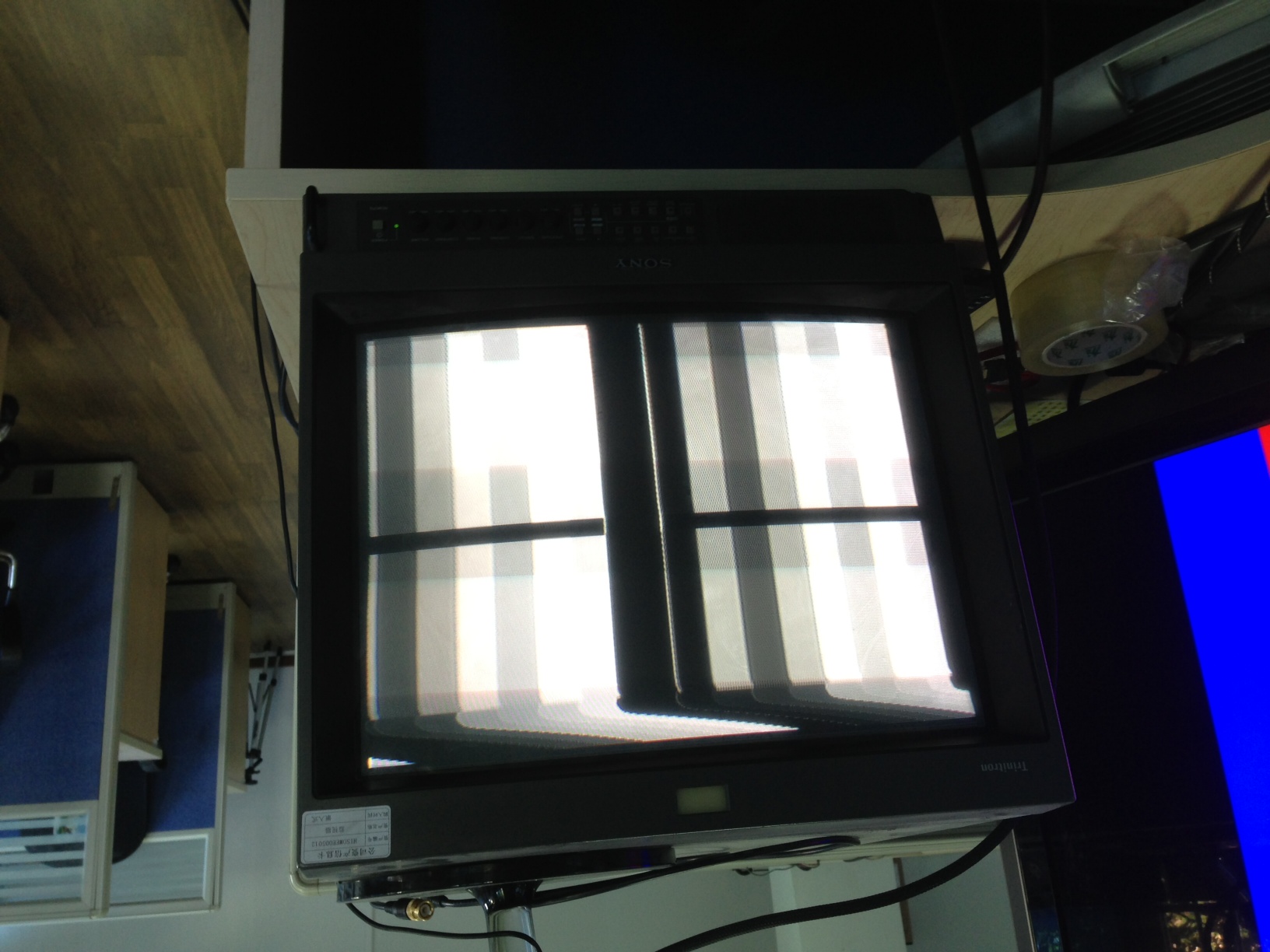
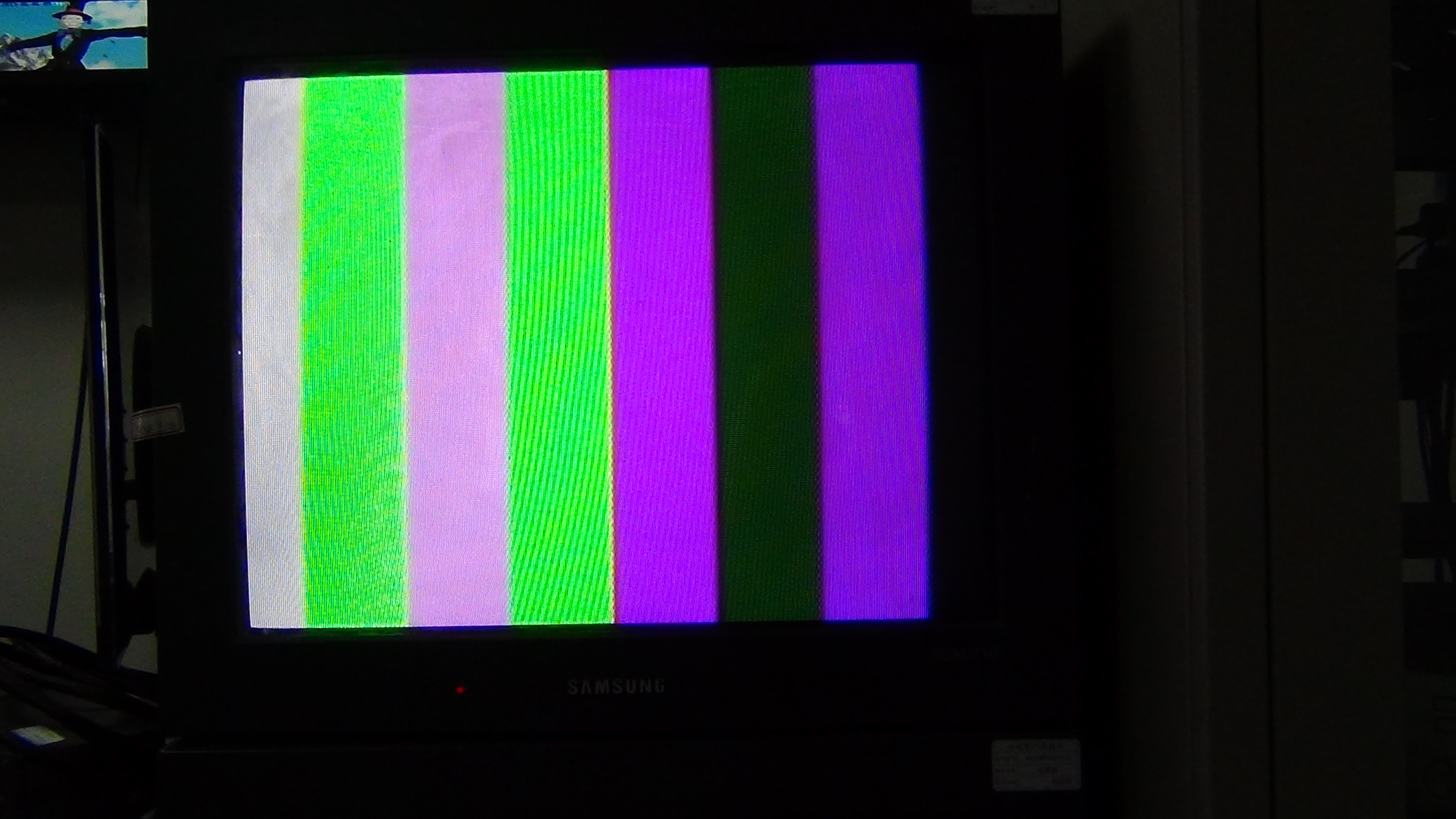
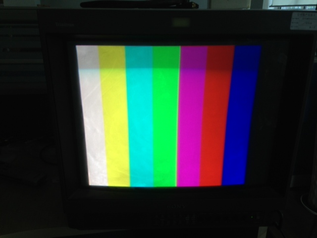
    I'm trying configure DM8167's DVO2 to output 576i video format with BT.656 to SAA7121, and let it output PAL analog video signals;

    I'm using DVRRDK_03.50.00.05, and modified following codes:

    mcfw/interfaces/ti_vdis_timings.h
        +/*<<CEA_Standard.pdf>> Pg.38: 4.10 720(1440)x576i@50Hz*/
        +#define VDIS_TIMINGS_PAL        "27000,720/12/69/63,576/2/19/3,0"

        +#define VDIS_SYSFSCMD_SET_OUTPUT      "/sys/devices/platform/vpss/display%d/output"
        +#define VDIS_OUTPUT_8BITS                "single,yuv422spuv,0/0/0/0"
        +#define VDIS_OUTPUT_16BITS                "double,yuv422spuv,0/0/0/0"


    mcfw/src_linux/mcfw_api/ti_vdis.c : Vdis_setResolution()

        +                    case VSYS_STD_PAL:
        +                        Vdis_sysfsCmd(3,VDIS_SYSFSCMD_SETTIMINGS, VDIS_SYSFS_DVO2,  VDIS_TIMINGS_PAL);
        +
        +                    break;

        ......

        +                switch(resolution)
        +                {
        +                case VSYS_STD_PAL:
        +                    Vdis_sysfsCmd(3,VDIS_SYSFSCMD_SET_OUTPUT, VDIS_SYSFS_DVO2,VDIS_OUTPUT_8BITS);
        +                    break;
        +
        +                default:/*1080P60,......*/
        +                    Vdis_sysfsCmd(3,VDIS_SYSFSCMD_SET_OUTPUT, VDIS_SYSFS_DVO2,VDIS_OUTPUT_16BITS);
        +                    break;
        +                }

My question:

    A. Is VDIS_TIMINGS_PAL correct?

    B. Does DVRRDK support PAL setting on DVO2? If not, which part of codes should to modify to support it?

Thanks a lot!

enigma<enigma0702@gmail.com>

2013-6-2

  • Hi,


    HDVPSS should also support PAL settings. Please use below link to get the settings for the PAL mode for DVO1/2 output.

     http://e2e.ti.com/support/dsp/davinci_digital_media_processors/f/717/p/230439/809857.aspx#809857


    Regards,

    Brijesh

  • I will try your link first, thanks a lot;

    enigma

    2013-6-3

  • Hi Brijesh, I tried your way, but I still can't get correct BT.656/625i signals on DVO2, following is HD_VENC_D_VOUT0's register value, please help check which value is wrong

     [m3vpss ] CFG00(0x4810a000): 0x07e0b05c
     [m3vpss ] CFG01(0x4810a004): 0x003f0275
     [m3vpss ] CFG02(0x4810a008): 0x1ea500bb
     [m3vpss ] CFG03(0x4810a00c): 0x1f9901c2
     [m3vpss ] CFG04(0x4810a010): 0x1fd71e67
     [m3vpss ] CFG05(0x4810a014): 0x004001c2
     [m3vpss ] CFG06(0x4810a018): 0x00200200
     [m3vpss ] CFG07(0x4810a01c): 0x184c0c77
     [m3vpss ] CFG08(0x4810a020): 0x1c0c0c30
     [m3vpss ] CFG09(0x4810a024): 0x1c0c0c30
     [m3vpss ] CFG10(0x4810a028): 0x84271360
     [m3vpss ] CFG11(0x4810a02c): 0x3f150016
     [m3vpss ] CFG12(0x4810a030): 0x3f2d8081
     [m3vpss ] CFG13(0x4810a034): 0x00000137
     [m3vpss ] CFG14(0x4810a038): 0x00038338
     [m3vpss ] CFG15(0x4810a03c): 0x3f2d0090
     [m3vpss ] CFG16(0x4810a040): 0x00017000
     [m3vpss ] CFG17(0x4810a044): 0x00121150
     [m3vpss ] CFG18(0x4810a048): 0x03001121
     [m3vpss ] CFG19(0x4810a04c): 0x0300113a
     [m3vpss ] CFG20(0x4810a050): 0x0013e13a
     [m3vpss ] CFG21(0x4810a054): 0x3f2d0088
     [m3vpss ] CFG22(0x4810a058): 0x00017001
     [m3vpss ] CFG23(0x4810a05c): 0x00121150
     [m3vpss ] CFG24(0x4810a060): 0x03001121
     [m3vpss ] CFG25(0x4810a064): 0x0300412b
     [m3vpss ] CFG53(0x4810a0d4): 0x00000000

    Thanks a lot!

    enigma

    2013-6-4

  • Hi,


    What error are you seeing? Is the output image correct? which decoder connected to vout0 detecting bt656 output?


    Regards,

    Brijesh

  • We are using SAA7121 connected to DM8167's VOUT0;

    The register settings of SAA7121 are copied  from our DM6467T->BT.656/625i->SAA7121 Custom Board, which display OK;

    Picture:

  • I learned a macro VPSHAL_HDVENC_ADJUST_TIMING_FOR_SHIFT_ISSUE in vpshal_hdvenc.c, it applied to FVID2_SF_PROGRESSIVE now, should it apply to FVID2_SF_INTERLACED too?

  • No This flag is not required for interlaced mode. Let me check the settings again.


    Regards,

    Brijesh

  • Hi Brijesh:

    I using another register configures and let VOUT0 in self test mode(color bar), then get following screen shot

    It seems incorrect color bar color, which register is wrong?


    REG diffs:

    - [m3vpss ] CFG00(0x4810a000): 0x07e0b05c
    + [m3vpss ] CFG00(0x4810a000): 0x0420b05c
      [m3vpss ] CFG01(0x4810a004): 0x003f0275
      [m3vpss ] CFG02(0x4810a008): 0x1ea500bb
      [m3vpss ] CFG03(0x4810a00c): 0x1f9901c2
    @@ -8,21 +8,21 @@
      [m3vpss ] CFG07(0x4810a01c): 0x184c0c77
      [m3vpss ] CFG08(0x4810a020): 0x1c0c0c30
      [m3vpss ] CFG09(0x4810a024): 0x1c0c0c30
    - [m3vpss ] CFG10(0x4810a028): 0x84271360
    - [m3vpss ] CFG11(0x4810a02c): 0x3f150016
    - [m3vpss ] CFG12(0x4810a030): 0x3f2d8081
    + [m3vpss ] CFG10(0x4810a028): 0x842716c0
    + [m3vpss ] CFG11(0x4810a02c): 0x7e150016
    + [m3vpss ] CFG12(0x4810a030): 0x7e5a8105
      [m3vpss ] CFG13(0x4810a034): 0x00000137
      [m3vpss ] CFG14(0x4810a038): 0x00038338
    - [m3vpss ] CFG15(0x4810a03c): 0x3f2d0090
    + [m3vpss ] CFG15(0x4810a03c): 0x7e5a0120
      [m3vpss ] CFG16(0x4810a040): 0x00017000
    - [m3vpss ] CFG17(0x4810a044): 0x00121150
    - [m3vpss ] CFG18(0x4810a048): 0x03001121
    - [m3vpss ] CFG19(0x4810a04c): 0x0300113a
    + [m3vpss ] CFG17(0x4810a044): 0x00120150
    + [m3vpss ] CFG18(0x4810a048): 0x03001120
    + [m3vpss ] CFG19(0x4810a04c): 0x03001142
      [m3vpss ] CFG20(0x4810a050): 0x0013e13a
    - [m3vpss ] CFG21(0x4810a054): 0x3f2d0088
    + [m3vpss ] CFG21(0x4810a054): 0x7e5a0118
      [m3vpss ] CFG22(0x4810a058): 0x00017001
    - [m3vpss ] CFG23(0x4810a05c): 0x00121150
    - [m3vpss ] CFG24(0x4810a060): 0x03001121
    + [m3vpss ] CFG23(0x4810a05c): 0x00120150
    + [m3vpss ] CFG24(0x4810a060): 0x03001120
      [m3vpss ] CFG25(0x4810a064): 0x0300412b
      [m3vpss ] CFG53(0x4810a0d4): 0x00000000

    Thanks a lot!

    enigma

    2013-6-6

  • In data structure VpsHal_HdVencConfig, I'm not understanding these members:

        VpsHal_HdVencAnalogConfig               analogConfig;
        /**< Analog configurations */
        VpsHal_HdVencDvoConfig                  dvoConfig;
        /**<  Digital configuration */
        VpsHal_HdVencOsdConfig                  osdConfig;
        /**< OSd configurations */

    anyone help me?

    Thanks a lot!

    enigma

    2013-6-13

  • Hi enigma,


    there is no need to understand these structures, driver takes care of configuring it correctly,

    Your register settings looks correct, could you check which YUV422 format is supported by your decoder? is it YUYV YVYU. UYVY or VYUY?


    Regards,

    Brijesh Jadav

  • Hi Brijesh:

        I am using  VOUT0 in self test mode(color bar), I need checking VOUT0's register setting for BT656/625i output works fine first, then display normal decoded video data;

        My application is based on DVRRDK's VSYS_USECASE_MULTICHN_VDEC_VDIS, it works 1080P60,720P60,SXGA_60,XGA_60 resolutions;  but the last PAL got stuck;

    enigma

    2013-6-13

  • Hi Brijesh:

        - [m3vpss ] CFG10(0x4810a028): 0x84271360

        + [m3vpss ] CFG10(0x4810a028): 0x842716c0

        CFG10.pixels[11:0] should be 0x360(864=(288+1440)/2) or 0x6c0(1728=288+1440)?

    -----------------------------------------------------------------------------------------------------------------------

        - [m3vpss ] CFG11(0x4810a02c): 0x3f150016

        + [m3vpss ] CFG11(0x4810a02c): 0x7e150016

        CFG11.eq_wth[31:24] should be 0x3F(126/2) or 0x7E(126)?

    -----------------------------------------------------------------------------------------------------------------------

        - [m3vpss ] CFG12(0x4810a030): 0x3f2d8081

        + [m3vpss ] CFG12(0x4810a030): 0x7e5a8105

        CFG12.hs_wth[31:24] should be 0x3F or 0x7E? Same with CFG11.eq_wth[31:24]?

        CFG12.act_pix[23:12] should be 0x2D8(728=720+8) or 0x5A8(1448=720*2+8)?

        CFG12.h_blank[11:0] should be 0x81(129=63+69-3) or 0x105(261=126+138-3)?

    -----------------------------------------------------------------------------------------------------------------------

        - [m3vpss ] CFG15(0x4810a03c): 0x3f2d0090
        + [m3vpss ] CFG15(0x4810a03c): 0x7e5a0120

        CFG15.vout_hs_wd[31:24] should be 0x3F or 0x7E? Same with CFG11.eq_wth and CFG12.hs_wth?

        CFG15.vout_avd_hw[23:12]: should be 0x2d0(720) or 0x5a0(1440=720*2)?

    -----------------------------------------------------------------------------------------------------------------------

        - [m3vpss ] CFG21(0x4810a054): 0x3f2d0088
        + [m3vpss ] CFG21(0x4810a054): 0x7e5a0118

        CFG21.osd_hs_wd[31:24] should be 0x3F or 0x7E? Same with CFG15.vout_hs_wd/CFG11.eq_wth/CFG12.hs_wth?

        CFG21.osd_avd_hw[23:12] should be 0x2D0 or 0x5A0? Same with CFG15.vout_avd_hw?

    -----------------------------------------------------------------------------------------------------------------------

    Reference:  /*<<CEA_Standard.pdf>> Pg.38: 4.10 720(1440)x576i@50Hz*/

    -----------------------------------------------------------------------------------------------------------------------

    enigma

    2013-6-13

  • Hi Brijesh:

        I'm setting DVO2 to use hd_venc_a_clk, How should I to configure the clock for PAL:

        A: hd_venc_a_clk(27MHz)->clk2x(27MHz)

                                                         |->dvo2_clk(27MHz)

        B: hd_venc_a_clk(54MHz)->clk2x(54MHz)

                                                         |->dvo2_clk(27MHz)

        Then clk1x should be 27MHz or 54MHz in B case;

        Is A correct or is B correct?

    enigma

    2013-6-14

  • Still waiting help from TI

  • Does DM8167's DVO2 support 8-bit mode output BT656?

    I guess it has a problem to support this;

    Is any body help me?

    enigma

    2013-6-28

  • Thanks Chris Meng (孟海燕) ,Under she's help, We solved this problem;

    With following Register settings:

    [CortexM3_ISS_0] CFG00(0x4810a000): 0x4420305c
    [CortexM3_ISS_0] CFG01(0x4810a004): 0x003f0275
    [CortexM3_ISS_0] CFG02(0x4810a008): 0x1ea500bb
    [CortexM3_ISS_0] CFG03(0x4810a00c): 0x1f9901c2
    [CortexM3_ISS_0] CFG04(0x4810a010): 0x1fd71e67
    [CortexM3_ISS_0] CFG05(0x4810a014): 0x004001c2
    [CortexM3_ISS_0] CFG06(0x4810a018): 0x00200200
    [CortexM3_ISS_0] CFG07(0x4810a01c): 0x184c0c77
    [CortexM3_ISS_0] CFG08(0x4810a020): 0x1c0c0c30
    [CortexM3_ISS_0] CFG09(0x4810a024): 0x1c0c0c30
    [CortexM3_ISS_0] CFG10(0x4810a028): 0x84271360
    [CortexM3_ISS_0] CFG11(0x4810a02c): 0x3f150017
    [CortexM3_ISS_0] CFG12(0x4810a030): 0x3f2d8081
    [CortexM3_ISS_0] CFG13(0x4810a034): 0x00000137
    [CortexM3_ISS_0] CFG14(0x4810a038): 0x00038338
    [CortexM3_ISS_0] CFG15(0x4810a03c): 0x3f2d0090
    [CortexM3_ISS_0] CFG16(0x4810a040): 0x00018000
    [CortexM3_ISS_0] CFG17(0x4810a044): 0x00120150
    [CortexM3_ISS_0] CFG18(0x4810a048): 0x03002120
    [CortexM3_ISS_0] CFG19(0x4810a04c): 0x03001142
    [CortexM3_ISS_0] CFG20(0x4810a050): 0x0013e13a
    [CortexM3_ISS_0] CFG21(0x4810a054): 0x3f2d0088
    [CortexM3_ISS_0] CFG22(0x4810a058): 0x00018001
    [CortexM3_ISS_0] CFG23(0x4810a05c): 0x00120150
    [CortexM3_ISS_0] CFG24(0x4810a060): 0x03001120
    [CortexM3_ISS_0] CFG25(0x4810a064): 0x0300412b
    [CortexM3_ISS_0] CFG53(0x4810a0d4): 0x00000000
    [CortexM3_ISS_0] CLKC VidEnc ClkSel: 0x0008010d

    Some Registers Still has problem, We will continue debug them;

    Display Effect Picture:

    enigma

    2013-8-2

  • good to see it started working..


    I believe the only change required is clk2x should be set to 27MHz and clk1x to be 13.5Mhz. Correct?


    Regards,

    Brijesh

  • Hi Brijesh:

     Yes, That's the key!

    enigma

    2013-8-2

  • Dear Enigma, Brijesh,

    May I know how to configure clk2x to 27MHz? I think clk2x is an external clock. Which pin connects this clock source?

    Thanks in advance.

    B.R.

    OC

  • Hi OC,


    VENC has two input clocks input, clk2x and clk1x, typically for 16 bit or 24 bit output mode, it uses clk1x input clock for its operations. but for bt656 output, since luma and choma are interleaved on 8 bit output, it needs the two times and clock, in this case, it uses clk2x input and it should be 27MHz for D1 output. It still needs clk1x input, which must be half of clk2x input.


    Regards.

    Brijesh Jadav

  • Hi OC:

        SYSCLK13->HD_VENC_D_CLK

        SYSCLK15->HD_VENC_A_CLK

        Do you mean this?

    enigma

    2013-8-5

  • Hi OC,


    one of the SYSCLK13 or SYSCLK15 can be used for VOUT0 bt656 output and that needs to be configured for 27MHz clock.


    Rgds,

    Brijesh

  • Dear Brijesh,

    How to set clk2x and clk1x for 8bit CCIR656 on DVO2? (I use hdvpss_01_00_01_42)

    Is it right?

        //For clk2x
        vpllCfg.outputClk = 27000u;
        vpllCfg.outputVenc = VPS_SYSTEM_VPLL_OUTPUT_VENC_D;
        nRetVal = FVID2_control(
                                systemDrvHandle,
                                IOCTL_VPS_VID_SYSTEM_SET_VIDEO_PLL,
                                &vpllCfg,
                                NULL);

        //for clk1x
        vpllCfg.outputClk = 13500;
        vpllCfg.outputVenc = VPS_SYSTEM_VPLL_OUTPUT_VENC_A;
        nRetVal = FVID2_control(
                                systemDrvHandle,
                                IOCTL_VPS_VID_SYSTEM_SET_VIDEO_PLL,
                                &vpllCfg,
                                NULL);

    BTW, how to set clkSrc? (VPS_DC_CLKSRC_VENCD or VPS_DC_CLKSRC_VENCA?)

            clkSrc.venc = VPS_DC_VENC_DVO2;
            clkSrc.clkSrc = VPS_DC_CLKSRC_VENCD; //VPS_DC_CLKSRC_VENCA
            nRetVal = FVID2_control(
                             pDispTaskCtxt->dcHandle,
                             IOCTL_VPS_DCTRL_SET_VENC_CLK_SRC,
                             &clkSrc,
                             NULL);

    Thank you.

    Kuve

  • Hi Kuve,


    Only small change is required in your code


        clkSrc.venc = VPS_DC_VENC_DVO2;
            clkSrc.clkSrc = VPS_DC_CLKSRC_VENCD_DIV2; //VPS_DC_CLKSRC_VENCA
            nRetVal = FVID2_control(
                             pDispTaskCtxt->dcHandle,
                             IOCTL_VPS_DCTRL_SET_VENC_CLK_SRC,
                             &clkSrc,
                             NULL);


    Rgds,

    Brijesh Jadav

  • Dear Brijesh,

    I have fixed this issue and thank you for your hint.

    Kuve

  • Dear Brijesh,

    Does 480P output format (CCIR656 on DVO2) support pixel clk 54000Hz output?

    I set vpllCfg.outputClk = 54000u, and print out

    [DM3] 243: Assertion @ Line: 609 in ti814x/src/vps_platformTI814x.c: 54000u != v
    pllCfg->outputClk : failed !!!

    If I want to 54000Hz pixel clock, how do I set vpllCfg?

    Thank you.

    Kuve

  • I see some note in vps_platformTI814x.c.

    Work around for the hardware bug where it failed to set
    54k frequency with generated with the values generated by
    getdivider function - Essentially m = 540 and M2 == 10 will not
    work

    I am not sure whether clk can't be set 54k.

    Could I modify this function Vps_platformTI814xSetVencPixClk in vps_platformTI814x.c and not to check != 54000u?

        if (VPS_SYSTEM_VPLL_OUTPUT_VENC_RF == vpllCfg->outputVenc)
        {
            GT_assert( GT_DEFAULT_MASK, 54000u  == vpllCfg->outputClk);
        }
    //    else if ((VPS_SYSTEM_VPLL_OUTPUT_VENC_A == vpllCfg->outputVenc) ||
    //            (VPS_SYSTEM_VPLL_OUTPUT_VENC_D == vpllCfg->outputVenc))
    //    {
    //        GT_assert( GT_DEFAULT_MASK, 54000u != vpllCfg->outputClk);
    //    }