This thread has been locked.

If you have a related question, please click the "Ask a related question" button in the top right corner. The newly created question will be automatically linked to this question.

QUESTIONS on 6678 PCIe multi message msi dma and inbound translation(steven ji help me!!!)

I'm working on my board which has 6678(RC) and v6 FPGA(EP) connected with pcie.  

We are working on this kind of unnormal type that Dsp will send some memory write packets to FPGA via pcie to start a DMA write from FPGA to DSP. This is success. 

1. first  i have a question about the inbound and bar confirgure.

in the DSP(RC)  

my bar1 base address is  0x90000000;

outbound low address is 0x90000000;(32bit type)

inbound low address is 0x10000000;

inbound offset   0x0;


as in the fpga side ,we cannot configure something like outbound address,

we made the address on line start from 0x90000000;

so,I can transfer the data from ep to my ddr3 in dsp side directly(0x90000000-0x10000000+offset);


I don't quite understand the original example

ibCfg.ibBar = PCIE_BAR_IDX_M; /* Match BAR that was configured above*/
ibCfg.ibStartAddrLo = PCIE_IB_LO_ADDR_M;(0x90000000)
ibCfg.ibStartAddrHi = PCIE_IB_HI_ADDR_M;
ibCfg.ibOffsetAddr = (uint32_t)pcieConvert_CoreLocal2GlobalAddr ((uint32_t)dstBuf.buf);//0x80000000;//
ibCfg.region = PCIE_IB_REGION_M;

using this configure ,i thought i should  find the data transfered from fpga in the 0x10800000 part ,but i still find it in the 0x00800000 part 

?why ?  also, if i name the offset as 0x80000000, i cannot find the data in the ddr3.

i know the offset is not a 32bit data,  but which fields are the actually offset  address used ?

and is my configure of the inbound translation right?(although i can receive the data successfully)


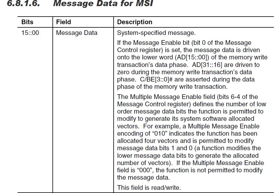
2. MSI (multi message)

 I've check some old posts about this, but they are all between dsps.

i want to use two message events, one for dsp to trigger a dma (fpga write to dsp ), one for dsp to know the completion of dma.

what should i do?

now, this is the situation:

i configure the bar0 in DSP(rc)  as base address (0x70000000) .

In the FPGA side ,it has such a function, which will send a message after the dma, i configure the MSI_DATA to 0x00000000,and low address to 0x70000054( so the fpga will send a pcie packet with its address set as 0x70000054).

actually, i've kind of receive this interrupt. But i don't quite get what i want and i 've some questions about this:


a. can I succeed to send two interrupts to dsp and how will i handle this?

   i know the msi interrupt event number is 17 in the primary interrupt event table, do the 32 msi events  share this ?and i can only have one hwi isr for it?   how can  do different things to different event?

b. I learned that to trigger a  msi interrupt , i should write data to the  MSI_IRQ in RC, what's the detail?

     as we know that we have 8 MSI_IRQ_STATUS and MSI_IRQ_ENABLE_SET registers , as i break in the hwi_isr, i will see the MSI0_IRQ_STATUS become 1 but  i see nothing changed  in the MSI_IRQ and IRQ_EOI  during the full process including interrupt status clearing.

    I was trying to add a MSI1 event to trigger the dma start, I've enable the multi_message_enable field , set the MSI1_IRQ_ENABLE_SET ,    it seems we enter the hwi ( and i move the dma in hwi,which will trigger the dma again at the end), but i see nothing changing  in the MSI1_IRQ_STATUS, the MSI_IRQ does not change too.

c. cfg file, anything to focus on?

this is my hwi configure in the cfg file following the old posts

var PCIeMSI_HwiParams = new Hwi.Params();
PCIeMSI_HwiParams.instance.name = "PCIeMSI_Hwi";
PCIeMSI_HwiParams.arg = 1;
PCIeMSI_HwiParams.enableInt = false;
PCIeMSI_HwiParams.eventId = 17;
PCIeMSI_HwiParams.priority = 4;
Program.global.PCIeMSI_Hwi = Hwi.create(5, "&hwi_isr", PCIeMSI_HwiParams);

d. because i don't see much multiple message interrupt  example, i want to have some details on this , i'm not sure you can understand what i say quite well, because  i 

am puzzled myself. anyting to add or make clear of my deomonstration, please let me know!


and I will appriciate if  anyone can help me on this!


  • 1. In the original example, I think your understanding is correct. Could you confirm you are using the example on Core0 or other cores please? 0x10800000 is only for Core0 L2, but 0x00800000 is the local L2 for every core.

    And bits[7:0] of IB_OFFSET register are reserved as you can see if the PCIe user guide. It seems fine to have 0x8000_0000 as offset. But I am not sure if anything else changed. Could you please check IB registers (IB_Start_Lo/HI, IB_Offset, IB_BAR0) directly to see what values are being programmed please?

    In your own inbound translation, the formula is correct that you could change either inbound LO/HI address or change inbound offset to map the incoming packets to the destination location.

    So you can also program IB_START_LO=0x90000000 (matches incoming PCIe address from FPGA) and program IB_OFFSET=0x80000000.

    But it is not recommended to have outbound address in RC to be the same as incoming PCIe address from EP (outbound address from EP, 0x90000000 in your example).  It will be better to have different outbound addresses in RC and EP and different BARn addresses in RC and EP (if you prefer to use BAR in RC, which is optional, please refer to BAR registers section in PCIe user guide for details).


    2. a

    PCIExpress_MSI_INTn is connected to CorePac_n in C6678, which means MSI_0 is connected to Core0 and MSI_1 is connected to Core1, etc.

    In each MSI event, there are four vectors such as MSI_0 includes MSI vectors 0,8,16,24. Once you receive the MSI event, in the ISR, you could check the bits in MSI0_IRQ_STATUS register to check which vector has been used in this event. You can set 1 to bits of MSI_IRQ to trigger MSI interrupt with different vectors, such as write 0x0 to trigger MSI vector0 and write 0x100 to trigger vector 8.

    2.b

    As we mentioned above, you should set corresponding bits in MSI_IRQ to trigger MSI interrupt. If you are using Core0 only in your case, you should set bits 0,8,16 or 24 in MSI_IRQ to trigger the MSI_0 interrupt. MSI_1 is not corrected to Core0, so it seems you are still triggering MSI_0 in your case (not MSI_1 event, so nothing changed in MSI1_IRQ_STATUS).

    2.c and d

    The HWI cfg setup seems fine and you are able to trigger the interrupt.

    The thing is missing that you can try to write different values in MSI_IRQ to trigger different vectors in MSI_0 for Core0 (if it is your case). As we mentioned above, you can check MSI0_IRQ_STATUS to see which vectors is being used and do the actions accordingly.

    Hope it could help.

  • Thank you Steven Ji.

    1.about the translation,I'll test for more.

     a. I have been operating on core0, as you say ,the offset only use   bits[7:0], so what's the different between  0x10800000 and 0x00800000? (while using 0x80000000, i can find nothing after the data transation)      

     b. But why  is it not recommended to have outbound address in RC to be the same as incoming PCIe address from EP?

    2. I've found out that I can only handle MSI 0,8,16,24 in core0, and we might have some mistakes in the early test. It's very awkward.

        But we have such a problem now.

       while i use 00 to trigger the msi0, i can break into the hwi_isr, but it seems always run twice!  

       my hwi_isr mainly include:

       msiIrqStatus[0].msiIrqStatus =0x1;

       irqEOI.EOI=0x4;

      by setting these two reigsters (using Pcie_write Regs), i think i can clear the status of the interrupt, but why?  run twice?


      so , I add the following code:

     Hwi_clearInterrupt(5);

    Hwi_enableInterrupt(5);

    It seems to solve the problem ,  one interrupt only triggers  hwi_isr once, but  for further msi0 interrupts, I can see the msi0_irq_status become 1, but the hwi_isr is not triggered.

    I don't see the old post use these code:

     Hwi_clearInterrupt(5);

    Hwi_enableInterrupt(5);

    is there any mistake? and where should i check my code.

    Thank you very much!!


  • 1.a

    Please take a look at section 3.1.85 in PCIe user guide that I mentioned bits 7:0 are Reserved (not being used) in IB_OFFSET. Bits [31:8] will take effect.

    You may want to check the IB_OFFSET_n (for IB_OFFSET0, it is 0x2180030c) values in the memory view to double check it is indeed the same as you plan to program. You can check the IB_STARTn_LO/HI and IB_BARn as well.

    If they look fine, you may want to further check the BAR setup/BAR mask (window size) and PCIe address over the link to see if the PCIe address is out of the region of BAR window.

    1.b

    Normally there could be multiple EPs connected to RC in PCIe hierarchy and the BARs (acceptable PCIe address region) of all the EPs should be OUTSIDE of the acceptable PCIe address region of RC. Otherwise the PCIe packets with PCIe address will match both RC and EP BARs (if you use BAR in RC) which will be confusing.

    In your case, if you have the same outbound address of RC and EP, which  means you need to have same BAR setup in RC and EP (since you use BAR in RC). It might be OK in the peer-to-peer transfer, since you only have one EP. But if you have another EP (EP2) and tries to send data to RC, the same data may be accepted by the other EP(EP1) as well since EP1 and RC has the same BAR setup. So it is recommended not to use the same setup for RC and EP outbound transaction.

    I think the PDK PCIe example, we are using different setup for RC and EP such as 0x90000000 and 0x70000000.

    2.

    In the ISR, besides clearing the interrupt status at source level (PCIe in this case), we may need to clear the CorePac INTC event as well.

    Below is the CSL example we could add to the ISR:

    /* Clear the CorePac interrupt */
    CSL_intcHwControl(hIntc,CSL_INTC_CMD_EVTCLEAR,NULL);

    For BIOS, I am not quite sure. Maybe you could only add "Hwi_clearInterrupt(5);" to see if it could re-trigger the same event.

  • Thank you ! Steve

    1. I've been beset by the problem for too long and totally forgot the main purpose of the address translation.

    2.I'll check  your suggestion on ISR as soon as quickly, and response soon!

  • steven 

    I haven't able to check the answer yet, but i have a further question to ask

    if I only use core0 ,and  want to use msi 0 and msi 8, should i set   msiCap.multMsgEn to 1 or 3(mean 8)? 

    and  should i set the EP with the same multmsgen?

    Thanks !

  • Xing,

    I think the "MSI_CAP" register is most likely to be used by the OS PCIe driver during the enumeration. The driver could understand the capability of MSI interrupts in RC and EP based on this register and assign the MSI vectors to EPs accordingly.

    I guess in the embedded system (peer-to-peer setup without PCIe enumeration driver) it cold be fine to trigger multiple MSI interrupts even have this MSI_CAP with default setup (support 1 MSI interrupt only). But it is no harm to set this register to support multiple interrupt based on real application.

    You may want to give a try since I am not quite sure about this. It will be good to share your observation as well. Thanks.

  • hello steven

    I've check the second problem.

    following the post you have answer:

    http://e2e.ti.com/support/dsp/c6000_multi-core_dsps/f/639/p/209655/742933.aspx#742933

    I changed the procedures to clear interrupt status as below

    *Msi0_IRQ_status=(uint32_t )0x1;

    *irq_eoi=(uint32_t)0x4;

    both of the pointers are the register address, I write data directly, and leave out the Hwi_clearInterrupt and Hwi_enableInterrupt code.

    It works well, no going into hwr_isr twice ,no stoping triggered by further interrupt.

    It seems the LLD of PCie especially with PCie_writeRegs has some problem.

    and for question one, why should i write 0x100 to trigger vector 8?

     as

    "You can set 1 to bits of MSI_IRQ to trigger MSI interrupt with different vectors, such as write 0x0 to trigger MSI vector0 and write 0x100 to trigger vector 8."

    why write 0 to trigger vector 0? not write 1 ? the MSI_IRQ has 32bits ,each one represent a vector?

    It is a message data description in the PCI specification, which is referenced in the PCIe specification, I'm a little confused, I will try different config, but i am welcome for your 

    suggestions.

    it is in page 243 of this pdf:

    1016.PCI.Local.Bus.Specification.Revision.3.0.pdf

  • Steven

    I've found out the right way to trigger 0,8,16,24 vectors.

    we should write 0,8,16,24 directly to MSI_IRQ, and each vector will assert the 0 ,1,2,3 bit in MSI0_IRQ_STATUS, also , i have to enable the four vector in MSI0_IRQ_ENABLE_SET(0x0000000F).

    Problems solved ,Thank you ,Steven Ji 

    really appreciate!!!!!

  • Xing,

    Sorry for the previous confusion. And you are right that, for the MSI_IRQ register, we should write "VALUE" into this register to trigger the MSI interrupt. Not  each bit represents each MSI interrupt, but the data value written into the register represents the number of MSI interrupt.

    So just like the description in the UG, in order to trigger MSI 0, we should write 0x00000000 to this register, instead of 0x00000001. Similarly, to
    trigger MSI 31, we should write 0x0000001F to this  register, instead of 0x80000000.


  • dear Steven

    I've come across a new problem.

    while I am using the multiple message interrupt, first the FPGA will send a vector 8 interrupt, then i wll start a dma from FPGA by sending some packets to FPGA via pcie,

    then the when this pcie dma finished ,the FPGA will send a interrupt vector 0 to DSP, then the dsp is assumed to do some further execution of the data.  the duration of the

    dma is about 30us, and the next vector 8 interrupt will come after the first vector 8 interrupt  for 100us.

    but as my hwi_irs, i will check the msi0_irq_status register for 1 and 2.

    but as i see(put breakpoint in the hwi_isr) , first i recive a vector 8 , the msi0_irq_status becomes 2 ,and  the dma start , next time i check the register , the value is 3 , it recieve both interrupt. actually I can't hit a time the register is 1 with only a vector 0 interrupt.

    is it because the interrupt cannot tell two events about 70us interval? what can i do

  • Xing,

    I think the two subsequent interrupts (vector 8 and vector 0) will come in the interval of 30us, which is the duration of DMA transfer, right?

    Once you receive the first interrupt, your ISR should be simple and compact enough to be existed before the next interrupt happens, is it correct?

    And in your ISR, the current interrupt received will be cleared in PCIe module as follows, is it correct?

    *Msi0_IRQ_status=(uint32_t )0x1 or 0x2; (depending on interrupt event received)

    *irq_eoi=(uint32_t)0x4;

  • sorry 

    I've express it not clearly.

    The FPGA will send a vector 8 interrupt every 200us, at first DSP only recive a 8 vector and send some data to FPGA to start a DMA,  but then I will recieve the 0 vector(means FPGA has finished the transfer) and vector 8.

    It seems that  the interrupt handler just can't tell the two interrupt apart!

    and another  phenomenon

    from the Chipscope of the FPGA side, we  can see the internal time between the vector 8 interrupt packet(FPGA to DSP) and the data send back to FPGA vary between 400 FPGA cycle to 4000 cycle(it is not accepted).

    I only have one task, only have this interrupt !  the hwi_isr only include this data transfer and status clear! why would this internal time vary? the

  • Xing,

    It might be helpful if you could take time stamps on certain points to understand the timing of your data flow. Such as you could get Time_1 when vector 8 triggers DSP interrupt ISR, Time_2 when DSP exists ISR and Time_3 when vector 1 triggers ISR. You would see if 200us is realistic for the vector 8 and vector 1 arrival and if it is appropriate to have data transfer inside ISR.

    For the time interval variation, you could see which part causing it by using the time stamp on DSP/FPGA side as well. Hope it could help.