


HI,
I have questions about power boot sequence on AM3352 & TPS65910A3.
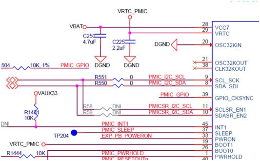
Below is a TPS65910A3 port of a starter kit. There, BOOT1 pin is connected to VRTC_PMIC and BOOT0 to GND.
TPs65910 seems to work differently according to the BOOT# pins. Does below diagram mean BOOT1=1/BOOT0=0 mode?
BTW, TPS65910 datasheet only describes BOOT1=0/BOOT0=0 mode & BOOT1=0/BOOT0=1 mode. There is no mention for BOOT1=1/BOOT0=0 mode. I quest it since the timing characteristic of 65910 varies depending on the boot mode.
My customer is designing following power rails.
VDDSSHV4(+1.8V) : is supplied from VDIG1 of TPS65910A3
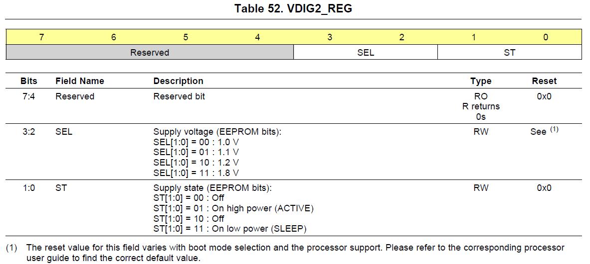
VDDSSHV6(+1.8V) : is supplied from VDIG2 of TPS65910A3
VDDSSHV1/2/3/5 (+3.3V) : is supplied from VMMC of TPS65910A3
SWIO is used for 1.5V DDR3 power.
SW1/2/3 should be specific values.
My question is about the voltage level.
For example, for 1.8V outputs in VDIG1 & 2 , SEL[1:0] should be configured at 11b. Can VDIG1/2 supply 1.8V when TPS65910 is powered? I don’t know well what user guide I should refer to for the default value. If the default value is fit for our use case, then should we use other power source?
Thanks,
Devin
