This thread has been locked.

If you have a related question, please click the "Ask a related question" button in the top right corner. The newly created question will be automatically linked to this question.

evm5515 - defining function (routing) for the SPI

Hi all,

I did not find the way to define the SPI lines routing to connector J13 (extension).

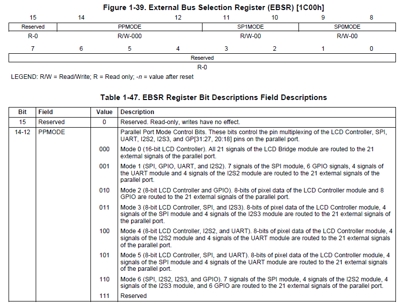
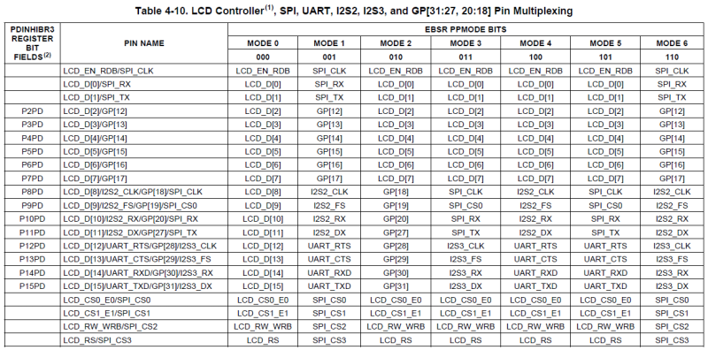
From the board schematics they are shared (including SPI_CS0) between LCD, SPI EPROM and Digital Extension header (J13),

but is not clear how to define the routing.

Thanks in advance for any suggestion,

Rubby

  • Hi Rubby,

    You select which peripherals are routed to the pins with the EBSR register (0x1c00).

    Sample CSL code: CSL_FINST(CSL_SYSCTRL_REGS->EBSR, SYS_EBSR_PPMODE, MODE1);

    You will see this sprinkled throughout the CSL exmaples.

    Hope this helps,
    Mark 

  • Hi Mark.

    This register defines the multiplexing inside the DSP,

    I am wondering about the routing the DSP' pins on the board -

    how to work with SPI on the connector J13 instead of SPI EPROM and how to disconnect the LCD and use these signals as SPI?

    Best,

    Roman

  • Hi Roman,

    The signals are all shorted with board traces and 0-ohm resistors, so only the EBSR controls where the SPI signals are routed on the board.

    With EBSR:PPMODE = MODE 1 or MODE 6, the only chip select muxed (SPI_CS0) goes to the LCD ribbon connector, not very easy without a ribbon cable

    EBSR:PPMODE = MODE 1/ MODE 6
    SPI_CLK = C5515:N3 = LCD_EN_RDB/SPI0_CLK = LCD_RE = SPI_ALT_CLK --- routed to P1:16 & J19:15
    SPI_TX = C5515:N6 = LCD_D[1]/SPI_TX = LCD_DATA1 = SPI_ALT_DX -------------- routed to P1:18 & J19:13
    SPI_RX = C5515:P6 = LCD_D[0]/SPI_RX = LCD_DATA0 = SPI_ALT_RX ------------- routed to P1:20 & J19:14
    SPI_CS0 = C5515:P4 = LCD_CS0_E0/SPI_CS0 = LCD_BIAS_OE --------------------- routed to J19:19
    SPI_CS1 = not routed to pins when PPMODE = 1 or 6
    SPI_CS2 = not routed to pins when PPMODE = 1 or 6
    SPI_CS3 = not routed to pins when PPMODE = 1 or 6

    With EBSR:PPMODE = MODE 3 or MODE 5, all SPI signals are available on the J13 header, but shared with the codec and EEPROM, so hold these devices in reset or make sure pins are Hi-Z to avoid contention. The other 3 chip selects are routed smaller connectors, but accessible.

    EBSR:PPMODE = MODE 3/ MODE 5
    SPI_CLK = C5515:N10 = LCD_D[8]/I2S2_CLK/GP[18]/SPI_CLK = LCD_DATA8 = I2S2_CLK = SPI_CLK -- routed to AIC3204_U12:2 & SPI_EEPROM_U9:6 & J13:3
    SPI_TX = C5515:P12 = LCD_D[11]/I2S2_DX/GP[27]/SPI_TX = LCD_DATA11 = I2S2_DX = SPI_DX ---------- routed to AIC3204_U12:4 & SPI_EEPROM_U9:5 & J13:11
    SPI_RX = C5515:N11 = LCD_D[10]/I2S2_RX/GP[20]/SPI_RX = LCD_DATA10 = I2S2_RX = SPI_RX --------- routed to AIC3204_U12:5 & SPI_EEPROM_U9:2 & J13:13
    SPI_CS0 = C5515:P11 = LCD_D[9]/I2S2_FS/GP[19]/SPI_CS0 = LCD_DATA9 = I2S2_FS = SPI_CS0 ------- routed to AIC3204_U12:3 & SPI_EEPROM_U9:1 & J13:7
    SPI_CS1 = C5515:N4 = LCD_CS1_E1/SPI_CS1 = LCD_MCLK = SPI_ALT_CS1 ---------------------------------- routed to P1:14
    SPI_CS2 = C5515:P5 = LCD_RW_WRB/SPI_CS2 = LCD_nWE -------------------------------------------------------- routed to J19:16
    SPI_CS3 = C5515:N5 = LCD_RS/SPI_CS3 ----------------------------------------------------------------------------------- routed to J19:20

    Hope this helps,
    Mark

  • Hi Mike,

    Thanks for fast and informative response.

    Only question - what is the way to hold codec and EEPROM in reset using the SW only?

    Thanks in advance,

    Roman