This thread has been locked.

If you have a related question, please click the "Ask a related question" button in the top right corner. The newly created question will be automatically linked to this question.

C6748 reset recovery issue

We are having an issue booting after we release the reset pin from a low state while the product is powered.  On our product we use a voltage detector to set the C6748's reset line low during power down and if there is a "brown out'.  The unit will recover fine if the main voltage is removed from the unit and re-applied.  But, if you bring the reset line low while all voltages are fine and stable, the unit will freeze during re-boot.  We have a 1K ohm pull-up from the /RST pin to 3.3V.  Also, we have a 4.75K ohm pull-down from the /TRST pin to ground.  I have varied the length of the reset pulse from milliseconds to 10+ seconds with the unit not booting.  Any thoughts?

  • Randy,

    I understood you’re facing some issue with POR (Power-On Reset) with the reset line low while all voltages are fine and stable the unit will freeze during re-boot. Hope you have a 1K ohm pull-up from the /RST pin to 3.3V.  Also, we have a 4.75K ohm pull-down from the /TRST pin to ground.

    Please follow the highlighted POR sequence hope that will fix your issue

    A power-on reset (POR) is required to place the device in a known good state after power-up. Power-On Reset is initiated by bringing RESET and TRST low at the same time. POR sets all of the device internal logic to its default state. All pins are tri-stated with the exception of RESETOUT which remains active through the reset sequence, and RTCK/GP8[0]. During reset, GP8[0] is configured as a reserved function,and its behavior is not deterministic; the user should be aware that this pin will drive a level, and fact maytoggle, during reset. RESETOUT in an output for use by other controllers in the system that indicates the device is currently in reset.

    While both TRST and RESET need to be asserted upon power up, only RESET needs to be released for the device to boot properly. TRST may be asserted indefinitely for normal operation, keeping the JTAG port interface and device's emulation logic in the reset state.TRST only needs to be released when it is necessary to use a JTAG controller to debug the device or exercise the device's boundary scan functionality. Note: TRST is synchronous and must be clocked by TCK; otherwise, the boundary scan logic may not respond as expected after TRST is asserted. RESET must be released only in order for boundary-scan JTAG to read the variant field of IDCODE correctly. Other boundary-scan instructions work correctly independent of current state of RESET. For maximum reliability, the device includes an internal pulldown on the TRST pin to ensure that TRST will always be asserted upon power up and the device's internal emulation logic will always be properly initialized.

    JTAG controllers from Texas Instruments actively drive TRST high. However, some third-party JTAG controllers may not drive TRST high but expect the use of a pullup resistor on TRST. When using this type of JTAG controller, assert TRST to intialize the device after powerup and externally drive TRST high before attempting any emulation or boundary scan operations.

    A summary of the effects of Power-On Reset is given below:

    • All internal logic (including emulation logic and the PLL logic) is reset to its default state

    • Internal memory is not maintained through a POR

    • RESETOUT goes active

    • All device pins go to a high-impedance state

    • The RTC peripheral is not reset during a POR. A software sequence is required to reset the RTC

    CAUTION: A watchdog reset triggers a POR.

    Please let me know if you have any further clarifications

    Regards

    Antony

    • --------------------------------------------------------------------------------------------------------
      Please click the Verify Answer button on this post if it answers your question.
      --------------------------------------------------------------------------------------------------------


  • Randy,

    When the C6748 comes out of POR, it will sample the boot configuration pins. In this case where the power is already stable and the device has booted once, are all of the config pins in the right state? If they are driven by other logic that does not get reset at the same time, then you might be booting up in the wrong state and/or the wrong boot mode.

    If you connect with JTAG, can you get control of the DSP and see where it is operating?

    Regards,
    RandyP

  • Thanks for getting back to me on this.

    The product has a LVDS LCD display so, we are using the boot config pins as LCD_Dx/Boot(x).  The pins are connected to a TI DS90CF3838 LVDS Transmitter ic.  On each of the config pins we have either a 1K pullup or pulldown.   Looking at each line while the reset is set low (via a momentary switch) and released, the lines either go low or high (depending on how they are pulled) and stay that way.


    Since I am a hardware guy, I will need to get one the software guys to try the JTAG idea.  Maybe tomorrow.


    Thanks,

    Randy

  • Hi RandyP,


    Had one of the software guys put the board on our JTAG fixture.  He said that the board comes out of reset but, does not start the boot loader.


    Thanks,

    Randy

  • Randy,

    Can you elaborate on that, please?

    What is the processor doing?

    What are the values in the BOOTCFG register in the good case and the failing case?

    Regards,
    RandyP

  • RandyP,


    Upon coming out of reset, the processor reads the boot config pins correctly to boot from SPI1 Flash and it hangs at that point.  From there, we cannot tell what the DSP is doing.


    Thanks,

    Randy

  • Randy,

    It sounds like the ROM Bootloader is doing what it is supposed to do.

    Are the SPI1 pins toggling after RESET is released?

    Does the SPI Flash need a reset to work?

    Is it a physical SPI Flash or an implementation in an FPGA or through a CPLD or any other logic?

    Regards,
    RandyP

  • Hi RandyP,


    The attached doc file contains what the SPI pins look like from a power boot up and when the reset line is released from a low state.  As you can see, we send and recv. data after reset for a few cycles but, nothing more. 

    The flash chip we are using is from Spansion (S25FL256AGNFI001) and that is being enabled by the DSP via /SPI1_SCSO..


    Thanks,

    Randy


    2402.SPI1 boot.doc


  • Hi,


    Checking in to see if anyone has anymore ideas.


    Randy

  • Hi,


    I take it that this has everyone stumped.


    Randy

  • Randy,

    We will check with the design team and get back to you

    Regards

    Antony

  • TI support team,

    We really need this question answered.  We are about to go "live" with this product, and don't have an answer for this problem.  We have other C6748 designs that don't have this problem (all boot from SPI FLASH as well).  The scope pictures that Randy shared pretty much explain the problem.  It looks like the TI ROM code attempts to access the SPI FLASH after a RESET, but then just stops for some reason.

    - Dean

  • Hi Dean

    What changed from your other c6748 design to this one? Same power circuit, same SPI flash, same speed for the SPI flash boot?

    What is the output of the debug GEL file

    http://processors.wiki.ti.com/index.php/OMAP-L1x_Debug_Gel_Files

    when the boot hangs?

    Regards

    Mukul

  • The power circuit is roughly the same, but slightly different.  However, the power rails satisfy the power up / power down sequence specified in the C6748 datasheet.  I see that the scope images Randy attached in the previous emails don't show the power rails with the RESET line, so I'll have him include that soon.

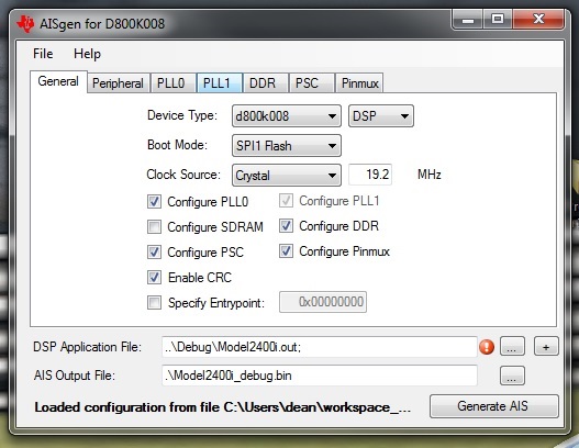
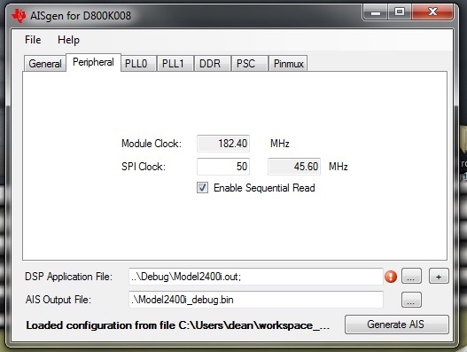
    The SPI FLASH is a different density, but from the same vendor.  The SPI boot speed is the same as the other projects.  I've attached snapshots of the AISGEN configuration information.

    We haven't tried a RESET on the emulator, as that screws up our environment.  However, I can tell you the Debug GEL file shows SPI1 as the boot method when we emulate normally.  In addition the scope images clearly show the TI ROM bootloader accessing the SPI FLASH after the RESET, so the boot pin have to be correct.  We are aware of the silicon errata that requires stronger pull up / pull down resistors on the boot pins.  We are using 1k resistors.

    - Dean

  • Dean

    The SPI clock speed seems to be much higher than what we typically support.

    There is a note in the boot loader application note(Pg 13)

    For SPI and I2C master modes, you can enter a desired speed. Depending on the PLL settings and
    granularity in peripheral clock division, AISgen calculates the actual speed nearest to the desired speed
    and shows it in an adjacent box. Recent I2C devices support speeds up to 400 kHz, and SPI devices
    support speeds up to 33 MHz

    Can you test with lower than 30 MHz SPI clock frequency.

    I would really like to see the supplies vs reset ramp, if reducing the clock freq  does not yield any clues. Since you confirmed that there is a change in the power circuit, the differences should be investigated on your working designs vs this board on what could be causing the difference.

  • >>However, I can tell you the Debug GEL file shows SPI1 as the boot method when we emulate normally.

    The debug gelf ile also gives us the program counter value for where the DSP is stuck, and lets us debug further where , if in RBL, is the code stuck.

    I do remember you being aware of the 1K pull up etc on the boot pins, it was your report and debug that led to generation of the device errata on this.

  • Hello Mukul,

    Please find the attached file that shows our power up, brown out, and power down sequence.  I have also added our power supply and reset circuit within the file.


    Regards,

    Randy

    2117.Power supply.doc

  • Hi Randy,

    In your design you are monitoring only the +5V power based on that you're releasing the reset pulse to the C6748 . You’re not monitoring the other power rails (3.3V, 1.2&1.8). Hope you have longer duration to release the reset pulse.

    We see the difference in the reset pulse duration during brown out condition (Reset and +5v during brown out and Reset and 1.25v, 1.8v, and 3.3v during brown out).

    Just be curious you need to monitor (3.3V, 1.2&1.8) rails connected to the C6748 device ,once these power rails gets stable then releasing the reset pulse become a valid one. How can you be sure every time if you do power ON/OFF or other brown out condition these rails  (3.3V, 1.2&1.8) are stable .Monitoring only the 5V power and releasing the reset with longer pulse duration will not always guaranteed. Some marginality in the (3.3V, 1.2&1.8) rails can cause you system to fail.

    Compare the Power/Reset scheme, power ramp Up/down waveforms in your working design and with the failing one and see the difference.

    Please share the results of brown out testing on your working/failing design for cross-reference.

    As mukul insisted have you tried on lowering the SPI clock frequency?

    Regards

    Antony

  • Mukul,

    We slowed the SPI clock in the AISGEN to 30.4MHz.  No luck.  I'm not sure why the ROM bootloader has a 33MHz limit, while the C6748 datasheet allows 50MHz.  Doesn't make a lot of sense.  By the way, if the ROM bootloader 33MHz limit is real, then the AISGEN program shouldn't allow you to enter a value greater than that.  Help us out where you can :)


    Antony,

    We should be perfectly fine just monitoring the +5V rail.  The brown out we generate never allows the +5V rail to go low enough that prevents the LDO (3.3, 1.8, 1.2) from regulating.  All three rails are rock solid.  In fact, we attempted to rule out the voltage detector RESET circuit and replaced it with a soft switch manual RESET.  Leaving the voltages alone (no brown out), and just applying a long (couple of seconds) manual RESET, still prevents the boot from happening.  Basically COLD RESET boots correctly, WARM RESET fails.

    I'm open for suggestions on what to try next.  We can supply a board if that will help.

    - Dean

  • Hi Dean,

    Have you tried Comparing the Power/Reset scheme, power ramp Up/down waveforms in your working design and with the failing one to see the difference.

    Please share the results of brown out testing on your working/failing design for cross-reference.

    Regards

    Antony

  • Antony,

    Yes we did compare the Power up / Power down / Reset waveforms between previous working products and our new one.  No difference.

    The good news, is we think we found the problem.  All our previous products used a SPI FLASH that was less than 16MB, and thus only required a 24bit address.  The C6748 bootloader document clearly says it requires a SPI FLASH that supports 24bit address.

    Our new product has 32MB of SPI FLASH, and the way we access all that FLASH space is to turn ON a bit inside the SPI flash so it requires 32bits addresses for reads and writes.  We had to write our own boot the bootloader application, so that the C6748 ROM only boots a small project, and then we continue booting after we've switched to 32bit addressing.  We completely forgot about this 24bit vs 32bit difference.  So what was happening, was the brown out was low enough to trip our DSP RESET, but now low enough to drop our 3.3V rail.  Because the 3.3V rail never dropped, the SPI FLASH never got a HW RESET, and thus was stuck in 32bit address mode when the C6748 ROM boot code attempted to access it using only 24bit addressing.  If the brown out was low enough (or power was completely removed), then the SPI FLASH would get its HW RESET, default back to 24bit addressing, and everything worked correctly.

    Thanks for the help.

  • Mukul,

    Can you please clarify the C6748 ROM requirement for SPI FLASH that it really has a 33MHz limitation.  We have always used 50MHz with no problems, and the C6748 datasheet clearly says it supports 50MHz.  If the 33MHz limitation is real, please explain why and update AISGEN so that values greater than 33MHz are invalid.

    Thanks, Dean

  • Hi Dean

    On further investigation on the comment on the boot loader application note, the 33 MHz is listed because this is what we had tested boot with few years back when the devices were announced. The bootloader author just wanted to capture the max/typical tested frequency.

    I did have another customer issue at ~ 50 MHz boot speed, but going through older threads, that ended up being a customer board problem.

    There are limitations with SPI slave boot mode speeds, but these are comprehended in the datasheet timings and companion boot wikis.

    50 MHz should work for boot too, as indicated in the datasheet timings for the device.So no change needed in your firmware for previously designed boards. I apologize for the confusion.

    In general, we do not burden the AISGEN GUI to generate error messages for out of bound frequencies, expectation is that the end user will look through the datasheet max limits and use the tools accordingly. We do provide additional ease-of-use tools in terms of the PLL calculator (which has been upgraded) to allow easier visualization and debug-ability.

    Hope this addresses your query. Good to see that you were able to identify the cause of failure on the brown out condition.

    Regards

    Mukul