This thread has been locked.

If you have a related question, please click the "Ask a related question" button in the top right corner. The newly created question will be automatically linked to this question.

AM335x GPMC problem

Other Parts Discussed in Thread: AM3359

Hi,

I have the following GPMC configuration on a AM3359 device (Silicon Rev 2.0):

- NOR Flash attached to CS0 of GPMC with multiplexed address/data bus (exactly as on the AM335x ICE board)
- MMU and cache enabled for memory except for NOR flash
- NOR flash is mapped to address 0x08000000

and the following code:


volatile
Uint16 *pmem16;

while(1==1)
{
  pmem16=(Uint16*)0x08000000;

  *(pmem16+0x00555)=0x00AA;
  *(pmem16+0x002AA)=0x0055;
  *(pmem16+0x00555)=0x0090;

  ManufacturerCode=*(pmem16+0x00000);
  DeviceCode=*(pmem16+0x00001);
  BlockProtectionStatus=*(pmem16+0x00002);
}


This code does put the NOR Flash into "AutoSelect" mode and reads manufacturer code, device code and block protection status of first block.
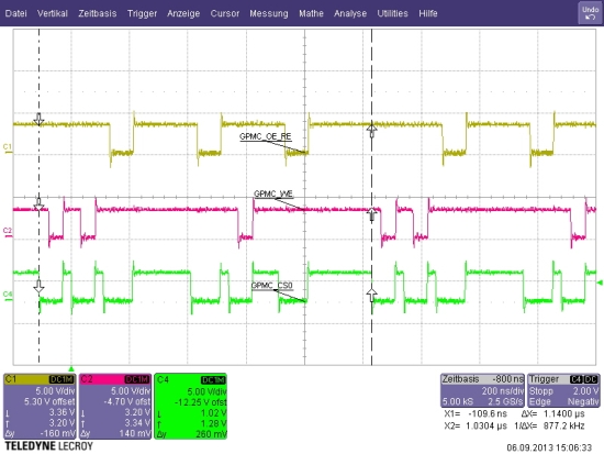
The code works fine if I step over the code in CCS and the signals on the scope look as they should.
But if I let the code run in an endless loop then three writes gets interrupted by some of the read operations and therefore the NOR flash does not switch into "AutoSelect" mode. How can I make shure that all the write operations to the NOR flash are all executed before the read operations are done?
Does this has to do with the L3 Slow Interconnect Interface and the pipelined interface?

Best regards,
Patrick

  • Hi Patrick,

    Did you take in concern the GPMC NOR memory timings? As it is external memory some timing constrains present on GPMC interface both for read and write?

    Several usecases are listed in the TRM 

    http://www.ti.com/general/docs/litabsmultiplefilelist.tsp?literatureNumber=spruh73i

    in section 7.1.4.1 How to Set GPMC Timing Parameters for Typical Accesses p.368.

    May be some delays between write and read operation can solve the problem.

    Hope this helps.

    BR,

    Vidin

  • Hi Vidin,

    Yes I did. Thanks. It is not a timing problem as far as I can tell. The problem is that the GPMC does not process the operations as they have been programmed. Means all the 3 write operations before the 3 read operations. If it is a timing problem, NOR Flash would not switch into "AutoSelect Mode" when I step over the code. Also the data read from NOR Flash is correct if I step over the code.

    Best regards,
    Patrick

  • Hi,

    The code I mentioned above translates into the following assembler code:

    80019108:   E3A01302 MOV             R1, #134217728
    8001910c:   E3002AAA MOVW            R2, #2730
    80019110:   E3A03055 MOV             R3, #85
    80019114:   E3004554 MOVW            R4, #1364
    80019118:   E3A050AA MOV             R5, #170
    8001911c:   E3A0E090 MOV             R14, #144
    80019120:   E1A0000C MOV             R0, R12
    80019124:   E1CDC0B0 STRH            R12, [R13]
    638         volatile Uint16 DeviceCode=0;
    80019128:   E1CD00B2 STRH            R0, [R13, #0x2]
    8001912c:   E3402800 MOVT            R2, #2048
    639         volatile Uint16 BlockProtectionStatus=0;
    80019130:   E1CD00B4 STRH            R0, [R13, #0x4]
    80019134:   E3A0C0F0 MOV             R12, #240
    663           *(pmem16+0x00555)=0x00AA;
              $C$DW$L$main$6$B, $C$L27:
    80019138:   E1C250B0 STRH            R5, [R2]
    664           *(pmem16+0x002AA)=0x0055;
    8001913c:   E18130B4 STRH            R3, [R1, R4]
    665           *(pmem16+0x00555)=0x0090;
    80019140:   E1C2E0B0 STRH            R14, [R2]
    671           ManufacturerCode=*(pmem16+0x00000);
    80019144:   E1D100B0 LDRH            R0, [R1]
    80019148:   E1CD00B0 STRH            R0, [R13]
    672           DeviceCode=*(pmem16+0x00001);
    8001914c:   E1D100B2 LDRH            R0, [R1, #0x2]
    80019150:   E1CD00B2 STRH            R0, [R13, #0x2]
    673           BlockProtectionStatus=*(pmem16+0x00002);
    80019154:   E1D100B4 LDRH            R0, [R1, #0x4]
    80019158:   E1CD00B4 STRH            R0, [R13, #0x4]

    I can see that the three writes (STRH ...) are all in the correct order. Then the three read (LDRH ...) follow as programmed. Why can I not see the three write operations on the GPMC signals in a row? Why are there read operations in between the write operations?
    What I see from the CS Signal (as the length is different in read and write) is the following: (please see scope picture below)

    1. Two write operations
    2. One read operation
    3. Wait for 320ns
    4. One read operation
    5. One write operation
    6. One read operation
    7. Wait for 220ns
    8. Repeat step 1

    Is there any queue between GPMC module, L3 Slow Interconnect and the ARM?

    What can I do to have the operations on the bus as programmed?

    The problem is getting urgent.

    Best reagards,
    Patrick

  • Hi Patrick,

    The Cortex-A8 does not necessarily read and write in-order.  There are no dependencies in your code. The reads do not depend on the writes, so the order should not be of concern.

    However,  that being said, there is a data memory barrier (DMB) instruction in the armv7 architecture which can be used to make sure all memory accesses before the DMB are completed before all the memory accesses after the DMB. This may impact the performance, but may be necessary in some situations.

  • Hi Jeff,

    Thanks for your answer.

    There are no dependencies in my code, your right. But there are dependencies in the NOR flash. The three write operations have to be in-order to switch the flash into a certain mode of operation. A read operation in between them does disturb this.

    However, this DMB command looks pretty interesting to me and could solve my problem...

    <Testing>

    I have just tried the "DMB" command and this works just great!

    Thanks Jeff

    Best regards,
    Patrick