Other Parts Discussed in Thread: TMS320C5515
Hello,
I have a custom board that's using a TMS320C5515 to talk to an 16 bit analog-to-digital converter, AD7665). Ideally, I'd like to run the SPI clock at 25MHz, however, the best I can do is 16.6MHz and below (clock divider of 6 using a 100MHz system clock).
The interesting thing I'm observing is that when I run the clock at 20MHz or 25MHz, the data captured by the DSP is shifted to the right by one bit. For example, I have a 3.3VDC applied to the ADC input, I would expect a binary value of approx 10,820. With clock rates at 20MHz and above, I capture values of approximately 5410, 1/2 of my expected value, or more importantly in binary,1 bit shifted to the right.
10,820 0010 1010 0100 0100
5,420 0001 0101 0010 1100
I was hoping for some insight to the TMS320C5515 clock tolerances (voltage levels/timing) on the SPI clock and data lines. I've gone through the SPI users guide (SPRUF03) and the DSP User's Guide, but can't find any info on this.
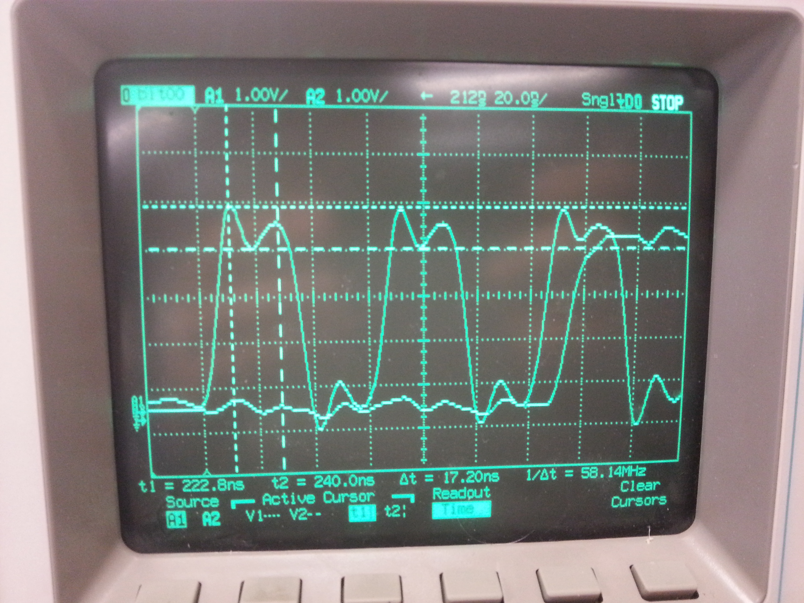
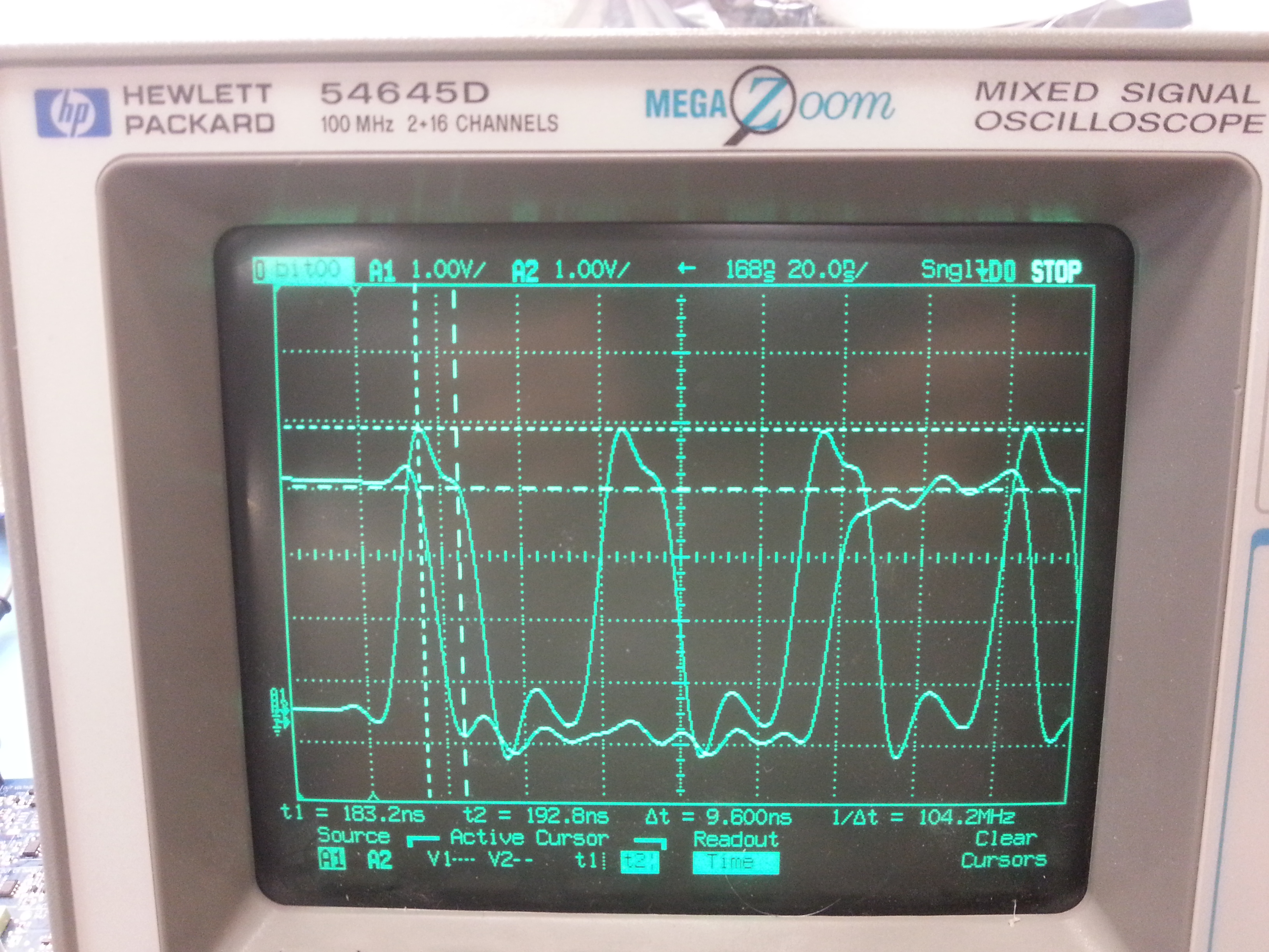
I've attached two screen shots of the first 3 bits (001) being clocked in, one of the 16MHz clock and one with the 20MHz clock. I know there's a bit of ringing on the line (which I think is partially due to my probe) but the ringing exists on the 16MHz side as well, which works.
The SPI is setup to receive data on the falling edge of the clock.
My background is more in software/firmware coding rather than hardware design, so I appreciate any insight you can provide.
Adam
16MHz clock: