This thread has been locked.

If you have a related question, please click the "Ask a related question" button in the top right corner. The newly created question will be automatically linked to this question.

C6678 SPI boot configuration

Other Parts Discussed in Thread: TMS320C6678

Hi,

I have questions on how to properly set  pull-ups and pull-downs on the GPIO in order to correctly configure SPI boot on 6678.

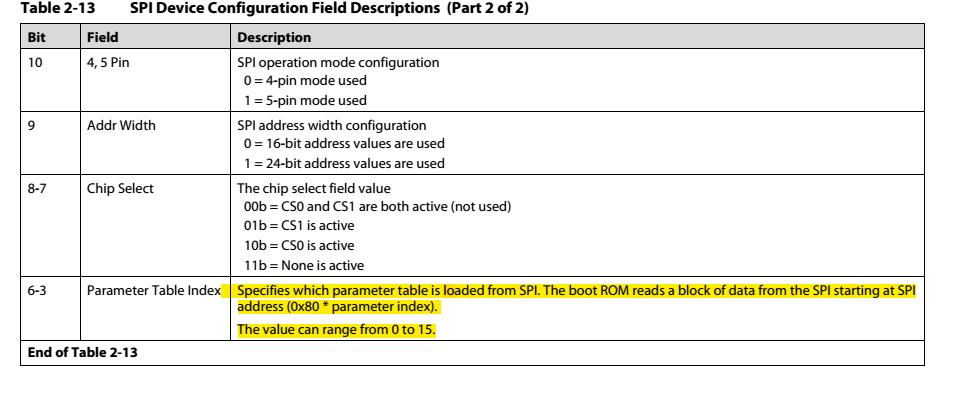
1)      As shown in table 2-11 of TMS320C6678 data manual, in the SPI booting device configuration setup section, Bit 8-7 is for chip select field value setup. Can somone point us which document we should look to find definition of those bits? My guess is that these two bits define which chip select to use, but since two bits define 4 numbers and there are two chip selects, which is proper value to select /CS0?

2)  I have an issue with Bits 6-3, parameter table index.  What is parameter table index? Where can I find the parameter table definition? I searched and searched all zillion pdf documents and I did not find the definition. Could someone point me to the document which I should read, or even better tell me what is proper configuration for those bits for SPI flash boot?

I wish TI pays more attention to documentation. In general, it is very poor with many things that are not explained well. I also suggest to group documenttion in much less pdf files, so it makes it easier to search. It is a pain in the a.. to search 150 pdf files. There should be hardware reference manual and programmers reference manual and that is it.

Thank you.

Gasha Gataric


  • 1.) I assume you mean Table 2-13 as that is the SPI Device Configuration for Boot Table, while Table 2-11 is for I2C Device Configuration.  Bit's 8-7 Correspond to SPICS[1:0]

    2.) The Boot Parameter Table is documented in the Boot Loader User Guide - http://www.ti.com/lit/ug/sprugy5c/sprugy5c.pdf

    There is a consolidated PDF of all Keystone Documents it's the 3rd major Link on the TMS320C6678 product page, right below the Data Sheet and the Errata.

    Best Regards,
    Chad 

  • Thank you for the replay but I did not any answer to my questions. Perhaps I was not clear what I do not understand.

    First, in the documat I have it is table 2-11 (document SPRS689D.pdf). This same table is duplicated in boot loader guide where it is labeled as Table 3-29 (SPRUGY5B.pdf). Second, I do know what is the name of those two bits, I do not know what values to use. For example a well written user guide would not say in the bit description:

    "0-3 = The chip select field value" (what the hack is field value?).

    Instead it would say:

    "0 - selects /CS0 for booting operation" (so it is clear that I have to connect /CS0 to the SPI flash CS for booting).
    "1 - selects /CS1 for booting operation"
    "2 - reserved for future use"
    "3 - reserved for future use"

    I do not know if there are other Keystone DSPs that have SPI interface with 4 chip select or not. So, I ask again, what number to put there if I have boot SPI flash connected to /CS0?

    Regarding my second question, the document you pointed out does not give me an answer either. There are four GPIO bits (GPIO4 to GPIO7)  that are read into "Parameter Index" field of SPI boot mode configuration register. The documentation says:

    "Parameter Table Index | 0-3 = Specifies which parameter table is loaded"

    How does that explain me what to do with the GPIO pins? Which should be pulled up and which should be pulled down? Do I need to have intimate knowledge how Code Composer Studio packs boot image for SPI flash booting in order to figure that one out? That is hopeless. I do not want to go into CCS details. All I want to know is how to pull-up / pull-down GPIO4 to GPIO7 bits that are mapped to SPI Device Configuration Field, bits 3 to 6 in order to have 6678 boot properly from SPI flash. Can anyone give me straight answer please?

    I am aware of what you called "consolidated file". I guess it depends what is you understanding of "consolidated". To me, putting a bunch of pdf file into a portfolio is not a consolidation. I still have to look through the list and try to figure out what document to open to find information I need. Very often the information I need is spread over multiple pdf files. I have to jump from one to another to put the picture together. For example, a single hardware reference guide would have one chapter dedicated to booting and all you need to know about booting would in that chapter. Just take a look into "Hardware User Manual" and "Programmers Reference Manual" of SHARC DSP. That is good documentation. TI has a long way to go to get there. It seems to me that each pdf file of TI documentation is written by different people. They do not talk to each other and sometimes one assumes that the other explained something so at the end there are things that are not explained well, like "The chip select field value" and "Parameter Table Index".

    Sorry for my frustrations, sometimes TI docs just drive me crazy.

    Gasha


  • Chad,

    The board manufacturing is on hold until these booting questions are resolved. I need answer on the questions above please. I also posted PLL / SPI clock frequency question in another thread. I would apreciate if I get answers asap.

    I long for good old days when it was possible to talk to support people and get answers in 5 minutes. If you are willing to give me a phone call, you can find my number in the TI customer data base: Slobodan Gataric, GE Aviation Systems. I could call you if you provide me a number.

    Thank you.

    Gasha


  • I assigned this question to another person that has a bit more expertise in the particular HW.  Hopefully he will be addressing it soon.

    Best Regards,

    Chad

  • I am eagerly waiting…

  • Slobodan,

    Sorry for the delayed response on this thread.There is a literature bug (SDOCM00103122)filed against this and we are working to resolve the issue. This is how the DEVSTAT bit line up for the SPI boot 

    DEVSTAT BITS
    13
    12
    11
    10
    9
    8
    7
    6
    5
    4
    3
    2
    1
    0
    Device
    Name
    Pll Config
    Device Configuration
    Boot Device
    Extended Dev Cfg
    PLL2
    PLL1
    PLL0
    Wait
    Width
    CS1
    CS0
    Sub-Mode
    rsvd
    0
    0
    0
    0
    ENDIAN
    Sleep
    EMIF16
    Lane
    Rate1
    Rate0
    R CLK1
    R CLK0
    Rsvd
    0
    0
    0
    1
    SRIO
    S CLK1
    S CLK0
    EXT1
    EXT0
    DevID2
    DevID1
    DevID0
    0
    1
    0
    ETHERNET
    1st block
    1st block
    1st block
    1st block
    1st block
    I2c
    0
    0
    1
    1
    NAND
    R CLK
    BAR3
    BAR2
    BAR1
    BAR0
    Rsvd
    0
    1
    0
    0
    PCIe
    0
    ADDR1
    ADDR0
    Speed
    Param5
    Param4
    Param3
    Param2
    Param1
    Param0
    1
    0
    1
    I2C Master
    1
    ADDR6
    ADDR5
    ADDR4
    ADDR3
    ADDR2
    ADDR1
    ADDR0
    Rsvd
    0
    1
    0
    1
    I2C Slave
    Mode1
    Mode0
    4/5 pin
    Addr Width
    CS1
    CS0
    Param3
    Param2
    Param1
    Param0
    1
    1
    0
    SPI
    PLL2
    PLL1
    PLL0
    rsvd
    Rate1
    Rate0
    R CLK1
    R CLK0
    Rsvd
    0
    1
    1
    1
    HyperLink
    speed
    speed
    parity
    parity
    port
    Rsvd
    1
    0
    0
    0
    UART

    Chip select 0 is picked by default from the boot mode pins which get latched to the DEVSTAT register as described in the data manual. The only values  0b10 (cs0 low) or 0b01 (cs1 low) are valid.

    For details, you can look at the tiboot.h file provided as part of the bootloader examples in the MCSDK 2.x ( \mcsdk_2_01_02_05\tools\boot_loader\ibl\src\device)or the source of the ROM code(section Keystone ROM Boot Examples and Reference code ) that we provide here :

    http://processors.wiki.ti.com/index.php/Keystone_Device_Architecture

    Following source will indicate to  you the relevant bits used by the ROM from the devstat register. This can be found in the file nysh.h in the ROM source. We are currently adding this information to the data manual.

    #define chipDefaultSpiPortNum()             0
    #define chipDefaultSpiPll()                 ((UINT32)(BOOT_PARAMS_PLL_CFG_CTL_NO_INIT) << (BOOT_PARAMS_PLL_CFG_CTL_SHIFT + 16))
    #define chipDefaultSpiOptions()             BOOT_PARAMS_SPI_OPTIONS_BP
    #define chipDefaultSpiAddrWidth()           (8 + (((readDevstatBits (10,10))+1) * 8))
    #define chipDefaultSpiNPins()               (4 + (readDevstatBits (11,11)))
    #define chipDefaultSpiCsel()                (readDevstatBits (9,8))
    #define chipDefaultSpiMode()                (readDevstatBits (13,12))
    #define chipDefaultSpiBusFreqMhz()          0      /* 2 MHz max */
    #define chipDefaultSpiBusFreqKhz()          500
    #define chipDefaultSpiReadAddr()            ((CHIP_WORDS_TO_BYTES(sizeof(BOOT_PARAMS_T))) * readDevstatBits(7,6))
    #define chipDefaultSpiNextCsel()            0
    #define chipDefaultSpiNextReadAddr()        0

    #define chipDefaultSpiC2tDelay()            1

    Regards,

    Rahul

    PS:

    You can also see the way the EVM boot pins are configured from the wiki below:

    http://processors.wiki.ti.com/index.php/TMDXEVM6678L_EVM_Hardware_Setup

  • Rahul,

    Thank you for the post. I am still missing something. The eval board (we have it by the way), has dip switches connected to the fpga so I do not know how the switches are connected to GIO pins through the fpga. Could you write down the mapping of the switches to GPIO bits? After you cleared up the values for CS bits, the only thing left is the parameter table bits.

    I really do not want to analyze boot loader code. Could you just tell me what these bits should be for SPI boot from NOR flash attached to CS0? if you give me the mapping of DIP switches I can figure it out from the eval board page you pointed to. Either way would work.

    You guys need to error proof documentation much better before you release it. It would save a lot of customer frustration. It does not give a good image to TI.

    Thank you.

    Gasha


  • Rahul,

    I got eval board schematic so I figured it out.

    One remaing question are GPIO bits 14 and 15.  The table have dip switches in "on" position which means GPIO pins are pulled low. In our design, we use GPIO14 and 15 as inputs that are by default driven high.  I could not find if those two bits matter for the SPI boot. If they do we have to add tristate buffers so we can have themn pulled low. If they do not, then there is no need to change anything.  Do they need to be pulled low for SPI boot?

  • Hi Slobodan,

    Thanks for the update and glad you could find the required hook ups. GPIO 14 and GPIO15 are not boot related switches. They are switches that select the the PCIESS mode0 and PCIESS mode 1 so unless you want to select a specific PCIE mode they, should be don`t care from boot perspective.

    Regards,

    Rahul

  • Thank you. I think that is al I need to make sure that the board will boot.

    Gasha

  • Hi Slobodan Gataric,

    I am a young engineer, my name is Frank Deng.

    I also met  the SPI boot problem in 6670. I am so crazy about TI documentaion!!!

    And I need your help, my question is posted here:

    http://e2e.ti.com/support/dsp/c6000_multi-core_dsps/f/639/p/288236/1013378.aspx#1013378

    http://e2e.ti.com/support/dsp/c6000_multi-core_dsps/f/639/p/297854/1038275.aspx#1038275

    The core quesion is the ROM version and how to config the boot parameter table and the boot config table. Our DDR is not working. Sooooooooo confused~~

    Allow me to express my apprecation advanced!

    Thanks a lot !

    Frank

    ---------------------------------------------------------------------------------
    Please click the
    Verify Answer button on this post if it answers your question.
    ---------------------------------------------------------------------------------

  • Frank,

    I am afraid I can not help you. I was part of the team that is working on the design of controller that uses 6678 dsp. I am a control engineer that does a little bit of hardware. I have another software engineer that looks into what it needs to be done so that the damn undocumented chip boots from SPI. He is having a lots of problems too. It has been two weeks since he started working on SPI booting using 6678 eval board. It still does not boot. I will talk to himn and see if he is willing to exchange information with you.

    Gasha 

  • Hi Frank,

    My name is Kevin Thayer. I am working on a project with Slobodan Gataric using the TMS320C6678. 
    We are only in our second week of trying to boot a simple application from the SPI flash on our
    evaluation board. A lot of this time has been spent reading posts from the forum along with conflicting
    information from the TI manuals. We still haven't had success. It frightens me that such an imperative
    process (booting from SPI flash) is so seemingly complicated by lack of clear documentation.
    I hope this is not the tip of the iceburg using this platform.

    Anyhow, it seems that you are much further along in the process than we are. We are still trying to boot a simple
    application on our EVM board from the SPI flash. We are not using DDR3 in our application. If you have
    any information that you could share with us to point us in the right direction, it would be greatly appreciated.

    Thanks,

    Kevin

  • Hi Kevin,

    Please refer to the document that I have attached that provides step wise instructions to create a boot image for SPI flash. Review the document and let us know if you still have issues.

    8304.Booting_from_SPI NOR_C6678.pdf

    Regards,

    Rahul

  • Rahul,

    Thanks for the information. Could you please post the SPI_Bootloader.zip file attachment separately (instead of embedded in the .pdf)?

    Thanks,

    Kevin

  • I have attached the simple LED blink example that is used with those instructions.

    4705.SPI_Bootloader.zip

    Hope this helps.

    Regards,

    Rahul

  • Gasha,

    Are you testing on an EVM borad provided by TI?

    Then you'd better make sure your EVM could be set to SPI boot mode.I have found my EVM6670 is hardware- setted to I2C boot, so the SPI boot cannot tested on the EVM.  Now I am testing on another board which is designed by ourself.

  • Rahul,

    I took the led_play.dat file from the .zip, renamed it to application.dat and burnt it into the EVM NOR flashfollowing the provided instructions. I then set the DIP switches as provided in the instructions as well. No success. A couple of questions:

    1.) Chip select DIP settings - the instructions in your file have both bits set to off. Previously in this thread, it has been stated that the only valid combinations are 0b10 or 0b01. Could you please elaborate? (I have tried all combinations with no success)

    2.) nysh.spi.map - sw_pll values - the evmc6678l.gel file has a table that states for the EVM settings of:

                          sw_pll_prediv = 1                      sw_pll_mult = 39                      sw_pll_postdiv = 2

          Do these values even matter for SPI boot when the PLL is supposed to be in bypass mode?

    3.) Also, the gel file has the core frequency listed as 1000 MHz for the evm.

    Thanks in Advance for your input,

    Kevin

  • Hi Kevin,

    I can feel you.I am glad to share with you, I have been frastrated struggling on SPI boot for 2 months and still have blocking issues.

    http://e2e.ti.com/support/dsp/c6000_multi-core_dsps/f/639/p/288354/1006025.aspx#1006025

    The above post may give you help, I made major progress from that one.

    The important thing is how to struct the parameter table and how to use the utilities. The second thing is how to config the DDR, it is not the (Address+SetCode+ClearCode) mode,but by a section built in to you application.

    Rahul Prabhu is the expert of this bootloader field, who helped me a lot.You can read my post and found his guide.

    Are you the big custom of TI? If so, ask you FAE to offer you more specified examples.

    Best wishes,

    Frank

    ---------------------------------------------------------------------------------
    Please click the
    Verify Answer button on this post if it answers your question.
    ---------------------------------------------------------------------------------

  • We are using the TMDSEVM6678LE Rev 3B evaluation board. The silicon revision for the DSP on the EVM is 2.0 (PLL issue at boot is supposedly fixed). I think from reading the wiki that I should be able to boot this particular EVM directly from the SPI flash. Haven't had any success so far though.

    Is this correct?

  • OK. Thanks Frank. First, I think you brought up an excellent point that we need to find out if our EVM board will even boot directly from the flash as per my most recent post. I had just assumed it would based on the silcon revision of the DSP.

  • Hi Kevin,

    Here is the update that we are trying to get into the documentation.

    So putting those chipselect to 00 should also work. this is not recommended as it has both chipselect enabled which could cause an issue if both chip selects are connected to a flash device but on EVM since only SPI_CS0 is used it should be ok to use.

    PLL configurations shouldn`t matter like mentioned as the device ROM bootloader will use the reference bypass clock. Core clock can be set to the value that you want the device to operate at.

    To debug the issue, can you run the debug GEL file and let me know where the Core0 program counter is at when the boot fails, also confirm the value in DEVSTAT corresponds to SPI boot.

    Even if the PLL sequence issue was fixed in the PG2.0 , the FPGA on the rev3 EVM still redirects the CPU to the I2C EEPROM before booting from the specified boot media. This was done to support all the boot modes on the EVM which may require some change in boot parameters before booting from the boot media.

    Regards,

    Rahul


  • Rahul,

    Thanks for the info. Since the NOR boot on the evm has to follow the IBL that is run from the i2c eeprom, does that mean that the DIP switches on the EVM should be configured for I2C Master boot and address 0x51 in order to boot from the NOR flash?

    Thanks,


    Kevin

  • For SPI boot, please set this to SPI boot settings BOOTMODE[2:0] =110. The example provided in MCSDK or  NOR boot which required the I2C settings.

    Regards,

    Rahul

  • Rahul,

    Still having trouble. The RBL appears to be stuck in a loop with PC values from 0x020B0CCD0 to 0x020B0CCD4. The DEVSTAT Boot Configuration value is always 0x00000A0B regardless of what boot mode is configured (except for No BOOT/EMIF). Below is information from the debug GEL:

    C66xx_0: GEL Output: *******************************************************************************************************

    C66xx_0: GEL Output: ********************************** C6678 BOOTSTRAP CONFIGURATION ******************************************************

    C66xx_0: GEL Output: *******************************************************************************************************

    C66xx_0: GEL Output: ********************************** C6678 Device Status Register (DEVSTAT) ************************************

    C66xx_0: GEL Output: BOOTCFG_DEVSTAT ---> 0x00000A0B

    C66xx_0: GEL Output: LENDIAN[0] ---> Little Endian

    C66xx_0: GEL Output: BOOTMODE[3:1] ---> I2C Boot Mode

    C66xx_0: GEL Output: SmartReflex ID[5:4] ---> 0

    C66xx_0: GEL Output: MODE[10] ---> Master Mode

    C66xx_0: GEL Output: ADDRESS[11] ---> Boot From I2C EEPROM at I2C bus address 0x51

    C66xx_0: GEL Output: SPEED[12] ---> I2C data rate set to approximately 20 kHz

    C66xx_0: GEL Output: PARAMETER IDX[9:4] ---> 32

    C66xx_0: GEL Output: PCIESSEN[16] ---> Initial state of the power domain and the clock domain for PCIE subsystem is Disabled

    C66xx_0: GEL Output: PCIESSMODE[15:14] ---> PCIE in End-point mode

    C66xx_0: GEL Output: PASSCLKSEL[17] ---> SYSCLK / ALTCORECLK (controlled by CORECLKSEL pin) is used as the input to PA_SS PLL

    C66xx_0: GEL Output: SYSCLKOUTEN[0] ---> No Clock Output

    C66xx_0: GEL Output: ********************************** C6678 DIEID Register (DIEID) ************************************

    C66xx_0: GEL Output: DIEID0 ---> 0x16004006

    C66xx_0: GEL Output: DIEID1 ---> 0x0403E8AE

    C66xx_0: GEL Output: DIEID2 ---> 0x00000000

    C66xx_0: GEL Output: DIEID3 ---> 0x16560021

    C66xx_0: GEL Output: ********************************** C6678 MACID Register (MACID) ************************************

    C66xx_0: GEL Output: MACID[31:0] ---> 0xEAC9F571

    C66xx_0: GEL Output: MACID[32:47] ---> 0x0017

    C66xx_0: GEL Output: BCAST[16](Broadcast Reception) ---> Broadcast

    C66xx_0: GEL Output: BCAST[17](MAC Flow Control) ---> Off

    C66xx_0: GEL Output: CHECKSUM[24:31] ---> 0x65


    C66xx_0: GEL Output: *******************************************************************************************************

    C66xx_0: GEL Output: ********************************** C6678 BOOT STATUS ******************************************************

    C66xx_0: GEL Output: *******************************************************************************************************

    C66xx_0: GEL Output: BOOTPROGRESS[31:0] ---> 0x2E011000

    C66xx_0: GEL Output: BOOTCFG_BOOTCOMPLETE ---> 0x00000000

    C66xx_0: GEL Output: C6678 Core 0 ---> Boot in process. Not Complete

    C66xx_0: GEL Output: C6678 Core 1 ---> Boot in process. Not Complete

    C66xx_0: GEL Output: C6678 Core 2 ---> Boot in process. Not Complete

    C66xx_0: GEL Output: C6678 Core 3 ---> Boot in process. Not Complete

    C66xx_0: GEL Output: C6678 Core 4 ---> Boot in process. Not Complete

    C66xx_0: GEL Output: C6678 Core 5 ---> Boot in process. Not Complete

    C66xx_0: GEL Output: C6678 Core 6 ---> Boot in process. Not Complete

    C66xx_0: GEL Output: C6678 Core 7 ---> Boot in process. Not Complete

    Any input you have would be greatly appreciated.

    Thanks,

    Kevin

  • Hi Kevin,

    It appears from the debug GEL log that your setting the EVM to I2C boot. Please set this to SPI boot. We have followed these steps and are able to boot the board into the application but sometime we don`t see the LED blink but the DSP has booted the code. So one test that you can perform is set the pins to SPI boot and connect the DSP core and you can see the PC is in MSMC region executing the code.

    Regards,

    Rahul

  • Rahul,

    I am setting the EVM DIP switch settings for SPI boot per the instructions you sent for the LED flash example. However, the GEL debug file is registering the DIP switches as I2C. This happens for all boot mode DIP switch settings except for NO BOOT/EMIF. Also, the PC appears to be caught in an infinite loop in the RBL address space (0x020B0CCD0 to 0x020B0CCD4). It seems like the RBL is "hung up" somehow and the IBL is never being executed?

    Note: the same thing happens if I try to run the I2C POST EVM boot. This morning I completely re-programmed my EVM board via the instructions and java script in the program_evm directory. The I2C POST EVM Boot mode still does not work. At this point I am really not sure what else to try but it seems that if I can't get the POST to work, the other modes are probably out of the question.

    Any input that you could provide would be most helpful.

    Thanks,

    Kevin

  • Hi Kevin,

    The boot mode switches on the EVM can be confusing. The EVM switches sometimes have the labeling done incorrectly. Please set the switch SPI boot mode using the settings provided on this wiki:

    http://processors.wiki.ti.com/index.php/TMDXEVM6678L_EVM_Hardware_Setup

    I checked the settings in that pdf with the one specified on the wiki and it appears where ever the pdf doc specifies 1 the switch settings need to be off.

    Regards,

    Rahul

  • Rahul,

    I have been setting the DIP switches per the Wiki. What is happening is that regardless of how I set the SW3 boot device bits (2,3,4), the debug GEL "C6678_Bootstrap_Configuration" script detects the boot mode as I2C and the SW3 nibble is detected as 0xB. To illustrate:

    Example 1: Power the EVM off and set DIP SW3 (1,2,3,4) to SPI boot (off, on, off, off). Power on the board and connect via CCS. Run the GEL "C6678_Bootstrap_Configuration" script -

    C66xx_0: GEL Output: BOOTCFG_DEVSTAT ---> 0x00000A0B

    C66xx_0: GEL Output: LENDIAN[0] ---> Little Endian

    C66xx_0: GEL Output: BOOTMODE[3:1] ---> I2C Boot Mode

    Example 2: Power the EVM off and set DIP SW3 (1,2,3,4) to Ethernet boot (off, on, off, on). Power on the board and connect via CCS. Run the GEL "C6678_Bootstrap_Configuration" script -

    C66xx_0: GEL Output: BOOTCFG_DEVSTAT ---> 0x00000A0B

    C66xx_0: GEL Output: LENDIAN[0] ---> Little Endian

    C66xx_0: GEL Output: BOOTMODE[3:1] ---> I2C Boot Mode

    So it seems that the EVM does not recognize the actual SW3 settings and hard codes them to I2C boot.

    Example 3: Power the EVM off and set DIP SW3 (1,2,3,4) to POST boot (off, off, on, off) from I2C address 0x50. Power on the board and connect via CCS. Run the GEL "C6678_Bootstrap_Configuration" script -

    C66xx_0: GEL Output: BOOTCFG_DEVSTAT ---> 0x00000A0B

    C66xx_0: GEL Output: LENDIAN[0] ---> Little Endian

    C66xx_0: GEL Output: BOOTMODE[3:1] ---> I2C Boot Mode

    C66xx_0: GEL Output: ADDRESS[11] ---> Boot From I2C EEPROM at I2C bus address 0x51

    So it doesn't choose the DIP switch address setting of 0x50 and nothing happens.

    Thanks,

    Kevin

  • Hi Kevin,

    I am going to close this older thread as we were able to resolve this issue by working with you offline.

    For benefit of those who refer to this thread in the future, the issue Kevin was facing was caused due to issue with the EVM caused due to faulty GPIO connections.

    Regards,

    Rahul

    PS: please start a new thread if you have any follow up queries.

  • hi Kevin, hi Rahul,

    where can I get this debug gel you are using?

    Thanks. Gregor

  • hi Kevin,

    fantastic! Thanks a lot. Really helpful information.

    I can see the correct boot mode and the successful completion now.

    Are there any more ways to see what the RBL is doing in real time, e.g how it is loading the words from NOR flash via SPI?

    Thanks+Regards.

    Gregor

  • I do not know of any troubleshooting tools for the RBL.

  • hi Kevin,

    in your post from October, 28th you mentioned:

    "The RBL appears to be stuck in a loop with PC values from 0x020B0CCD0 to 0x020B0CCD4."

    How could you see that?

    Thanks+Regards.

    Gregor

  • nobody any idea?