This thread has been locked.

If you have a related question, please click the "Ask a related question" button in the top right corner. The newly created question will be automatically linked to this question.

C6670(TMS320C6670CYP) SPI bootloader problems

Other Parts Discussed in Thread: TMS320C6670

Hi Rahul,

Thanks to your explaination on http://e2e.ti.com/support/dsp/c6000_multi-core_dsps/f/639/p/288354/1006025.aspx#1006025,     which helped me a lot to make progress.

But the boot progress have problems now. I would have missed something. And I eagerly need your help.

QUESTION  1, My RBL VERSION?

. My chip is TMS320C6670CYP,from the http://www.ti.com/product/tms320c6670 , it is say this Part# is OBSOLETE,

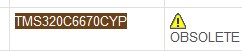
so, the Urgent problem is to make clear the ROM Bootloader version of this OBSOLETE chip  TMS320C6670CYP .  Because i found the parameter variable name of  your example nysh.spi.map  is different from the C6670 PG1.0 Bootloader.( http://software-dl.ti.com/sdoemb/sdoemb_public_sw/rbl/1_0_C6670/index_FDS.html

Please send the corresponding version RBL source code  to my email: denghengmin@126.com

for example, you can see the Different below,which means,the nysh.spi.map didnt matche the ROM parameter, or the C6670 PG1.0 Bootloader is not  the vertion of the TMS320C6670CYP RBL.

//////////////////////////////////////////////////////////////////////////////////////////////

the nysh.spi.map boot parameter struct is :

section {
 boot_mode = 50
 param_index = 0
 options = 1
 core_freq_mhz = 1000
 exe_file = "spiboot.i2c.ccs"
 next_dev_addr_ext = 0x0
 sw_pll_prediv = 5
 sw_pll_mult = 32
 sw_pll_postdiv = 2
 sw_pll_flags = 1
 addr_width = 24
 n_pins = 4
 csel = 0
 mode = 0
 c2t_delay = 0
 bus_freq_mhz = 0
 bus_freq_khz = 500
}

the  C6670 PG1.0 Bootloader tiboot.h is:

--------------------------------------------------------------

typedef struct boot_params_spi_s
{
    /* common portion of the Boot parameters */
    UINT16 length;
    UINT16 checksum;
    UINT16 boot_mode;
    UINT16 portNum;
    UINT16 swPllCfg_msw;  /* CPU PLL configuration, MSW */
    UINT16 swPllCfg_lsw;  /* CPU PLL configuration, LSW */
   
    UINT16 options;
     UINT16 addrWidth;          /* 16 or 24 are the only valid values */
     UINT16 nPins;              /* 4 or 5 pins are the only valid values */
     UINT16 csel;               /* only values 0b10 (cs0 low) or 0b01 (cs1 low) are valid */
     UINT16 mode;               /* Clock phase/polarity. These are the standard SPI modes 0-3 */
     UINT16 c2tdelay;           /* Setup time between chip select assert and the transaction */
    
     UINT16 cpuFreqMhz;         /* Speed the CPU is running after PLL configuration */
     UINT16 busFreqMhz;         /* The speed of the SPI bus, the megahertz portion */
     UINT16 busFreqKhz;         /* The KHz portion of the bus frequency. A frequency of 1.5 MHz would have the value 5 here */
    
     UINT16 read_addr_msw;      /* The base address to read from the SPI, upper 16 bits */
     UINT16 read_addr_lsw;      /* The base address to read from the SPI, lower 16 bits */
    
     UINT16 next_csel;          /* The next chip select to use if in boot config mode, when the config is complete */
     UINT16 next_read_addr_msw; /* The next read address to use if in boot config mode */
     UINT16 next_read_addr_lsw; /* The next read address to use if in boot config mode */
            
} BOOT_PARAMS_SPI_T;

//////////////////////////////////////////////////////////////////////////////////


[QUESTION 2] NEW romparse utilities available?

You explained here the romparse is not available to append the boot config table, is there any new update?

http://e2e.ti.com/support/dsp/c6000_multi-core_dsps/f/639/p/288354/1006025.aspx#1006025

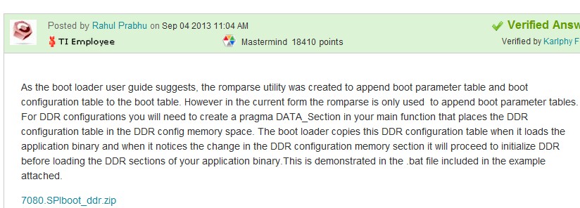
"As the boot loader user guide suggests, the romparse utility was created to append boot parameter table and boot configuration table to the boot table. However in the current form the romparse is only used  to append boot parameter tables. For DDR configurations you will need to create a pragma DATA_Section in your main function that places the DDR configuration table in the DDR config memory space. The boot loader copies this DDR configuration table when it loads the application binary and when it notices the change in the DDR configuration memory section it will proceed to initialize DDR before loading the DDR sections of your application binary.This is demonstrated in the .bat file included in the example attached."


[QUESTION 3]  How to  Config the DDR specified for 6670?

(Your example is not for 6670, and no documentation to refer to.)

The question is how to construct the DATA_Section , because I found the const BOOT_EMIF4_TBL_T  emif4Cfg={}  does NOT match the Bootloaser User guide(SPRUGY5B.pdf) 

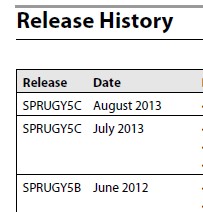
but unfortunately, SPRUGY5C.pdf totally cut this part, even if it claimed it is moved to the data manual ,but NOTHING updated to the 6670 data manual


Other users also rise this quesion:

http://e2e.ti.com/support/dsp/c6000_multi-core_dsps/f/639/p/288354/1006025.aspx#1006025 (see the last reply)

http://e2e.ti.com/support/dsp/c6000_multi-core_dsps/f/639/t/288236.aspx(see the last reply)


So ,which is the right DDR config struct?


Thanks a lot !

Frank

  • 1. Please send the RBL source code for my OBSOLETE chip  TMS320C6670CYP  to my mail :denghengmin@126.com.

    2.Please send the new romparse the the corresponding user guide and sourse code to my email, too

    3.If new romparse is still not available,please tell me the exact pragma DATA_Section and the exact BOOT_EMIF4_TBL_T  emif4Cfg  struct. to config the DDR specified for TMS320C6670CYP.(your example spiboot.h is not for 6670).

    4.Please check the boot parameter table which will be configed in your nysh.spi.map, is it for 6670?is the variablename all right for 6670?

    our project is blocked for a couples of weeks because the Bootloader is still a not stable situation.

    PLEASE PLEASE PLEASE PLEASE HELP ME...


    Thanks a lot!

  • Hi Frank,

    The device nomenclature is given in the data sheet in Figure 2-17.  If you don`t have the alphabet A between the part number and the package code (CYP) this is likely to be a silicon PG 1.0 version.

    One way to configure the DDR3 is by populating the DDR2 configuration table (bootEmif4Tbl_s) and load it as part of your application and place the structure  in the DATA_SECTION (emif4Cfg, ".emif4Cfg") as has been demonstrated in the example I shared with you. This process offloads DDR initialization to the boot ROM.

    If there are specific DDR initializations that the ROM doesn`t support you can use a second approach to perform this is by designing a 2 stage boot process where you boot into a main function where you configure the DDR and then re-enter the boot using the boot reentry address. When you renter Boot ROM , it will read not re-read the DEVSTAT or PLL settings but directly enter function to read the boot media and boot process.Your second stage boot can then load code into DDR space. To boot the second stage you will need to modify the read_addr_msw and read_addr_lsw in the SPI parameter table in the main function after configuring the DDR to read from the offset where you have written the second stage boot in your SPI NOR.

    For the second approach, the only example we have is the SRIO_DDRInit example in the MCSDK 2.x under tools/bootloader/examples/srio but it uses the IBL approach.

    Regards,

    Rahul


    PS: Please look at the reboot.c that I have attached. This was created for a 2 stage boot for ethernet boot but I have added some comments to elaborate the process.

    /*
     *
     * Copyright (C) 2011 Texas Instruments Incorporated - http://www.ti.com/ 
     * 
     * 
     *  Redistribution and use in source and binary forms, with or without 
     *  modification, are permitted provided that the following conditions 
     *  are met:
     *
     *    Redistributions of source code must retain the above copyright 
     *    notice, this list of conditions and the following disclaimer.
     *
     *    Redistributions in binary form must reproduce the above copyright
     *    notice, this list of conditions and the following disclaimer in the 
     *    documentation and/or other materials provided with the   
     *    distribution.
     *
     *    Neither the name of Texas Instruments Incorporated nor the names of
     *    its contributors may be used to endorse or promote products derived
     *    from this software without specific prior written permission.
     *
     *  THIS SOFTWARE IS PROVIDED BY THE COPYRIGHT HOLDERS AND CONTRIBUTORS 
     *  "AS IS" AND ANY EXPRESS OR IMPLIED WARRANTIES, INCLUDING, BUT NOT 
     *  LIMITED TO, THE IMPLIED WARRANTIES OF MERCHANTABILITY AND FITNESS FOR
     *  A PARTICULAR PURPOSE ARE DISCLAIMED. IN NO EVENT SHALL THE COPYRIGHT 
     *  OWNER OR CONTRIBUTORS BE LIABLE FOR ANY DIRECT, INDIRECT, INCIDENTAL, 
     *  SPECIAL, EXEMPLARY, OR CONSEQUENTIAL DAMAGES (INCLUDING, BUT NOT 
     *  LIMITED TO, PROCUREMENT OF SUBSTITUTE GOODS OR SERVICES; LOSS OF USE,
     *  DATA, OR PROFITS; OR BUSINESS INTERRUPTION) HOWEVER CAUSED AND ON ANY
     *  THEORY OF LIABILITY, WHETHER IN CONTRACT, STRICT LIABILITY, OR TORT 
     *  (INCLUDING NEGLIGENCE OR OTHERWISE) ARISING IN ANY WAY OUT OF THE USE 
     *  OF THIS SOFTWARE, EVEN IF ADVISED OF THE POSSIBILITY OF SUCH DAMAGE.
     *
    */
    
    /*
     *    Two stage boot example.
     *
     *    This code demonstrates a two stage boot procedure using the I2C as the
     *    pin strapped boot mode. The code reconfigures the ROM boot loader
     *    to execute a SRIO boot, performs PLL initializations that are required
     *    but not present in the boot ROM, then branches back into the ROM
     *    which performs the standard SRIO boot.
     */
    
    #include "tiboot.h"
    #include "ti/platform/evmc6678l/platform_lib/include/evmc66x_i2c_eeprom.h"
    
    #define	ETH_DEVICE_INIT
    
    
    /* Nyquist/Shannon boot modes */
    
    #define BOOT_MODE_PIN_SLEEP_EMIF25_SUBMODE_SLEEP   0
    #define BOOT_MODE_PIN_SLEEP_EMIF25_SUBMODE_EMIF25  1
    
    #define BOOT_MODE_ETH               10
    #define BOOT_MODE_RAPIDIO           20
    #define BOOT_MODE_PCIE              30
    #define BOOT_MODE_I2C               40
    #define BOOT_MODE_I2C_PASSIVE       41
    #define BOOT_MODE_I2C_MASTER_WRITE  42
    #define BOOT_MODE_SPI               50
    #define BOOT_MODE_VUSR              60
    #define BOOT_MODE_EMIF25            70
    #define BOOT_MODE_SLEEP             100
    
    /*
     *    ROM reboot configuration.
     *
     *    Adjust these parameters to match the platform
     */
    /* For SPI boot replace this with SPI parameter table */
    BOOT_PARAMS_ETHERNET_T boot_params =
    {
        sizeof(BOOT_PARAMS_ETHERNET_T),      /*  length *//*0x003E=62*/
        0,                                 /*  checksum *//*0x0000=0*/
        BOOT_MODE_ETH,                    /*  boot mode *//*0x000A=10*/
        0,                                 /*  port num *//*0x0000=0*/
        16400,							          /* SW PLL Cfg_MSW *//*0x4010=16400*/
    	  258,							            /* SW PLL Cfg_LSW *//*0x0102=258*/
    	BOOT_PARAMS_ETH_OPTIONS_RMII_10,                    /*0x0006=6*/
    	16479,										         /* Mac Addr Hi *//*0x405F=16479*/
      49856,                            /* Mac Addr Med *//*0xC2C0=49856*/
    	50772,                             /* Mac Addr Lo *//*C654=50772 DSP0=C654=50772, DSP1=C655=50773, DSP2=C656=50774,*/
    	65535,						/* Multi/Broad cast Mac Addr Hi *//*FFFF=65535*/
    	65535,			   	 /* Multi/Broad cast Mac Addr Med *//*FFFF=65535*/
    	65535,				 		/* Multi/Broad cast Mac Addr Lo *//*FFFF=65535*/
    	0,										           /* Source Port 0 *//*0x0000=0*/
    	9,									          /* Destination port *//*0x0009=9*/
    //	12336,									                            /*0x3030=12336*//* Device ID 1_2 ARUN MANI update: Change this ID to differentiate between the first bootp and the bootp after DDR init.*/
    	51966,									                            /*0xCAFE=51966*//* Device ID 1_2 ARUN MANI update: Change this ID to differentiate between the first bootp and the bootp after DDR init.*/
    	12336,										        /* DeviceID 3_4 *//*0x3030=12336*/
    	65535,										    /* Dest Mac Addr Hi *//*FFFF=65535*/
    	65535,										   /* Dest Mac Addr Med *//*FFFF=65535*/
    	65535,									      /* Dest Mac Addr Lo *//*FFFF=65535*/
    	16,										            /* SGMII Config *//*0x0010=16*/
    	32,									             /* SGMII Control *//*0x0020=32*/
    	38913,										/* SGMII MR_ADV_Ability *//*0x9801=38913*/
    	1,									        /* SGMII TX Config Hi *//*0x0001=1*/
    	2209,									     /* SGMII TX Config Lo *//*0x08A1=2209*/
    	112,									     /* SGMII RX Config Hi *//*0x0070=112*/
    	1569,									     /* SGMII RX Config Lo *//*0x0621=1569*/
    	0,									      /* SGMII AUX Config Hi *//*0x0000=0*/
    	129,									    /* SGMII AUX Config Lo *//*0x0081=129*/
    	32789,							   		    /* Pkt PLL Cfg MSW *//*0x8015=32789*/
    	258,									      /* Pkt PLL Cfg LSW */	 /*0x0102=258*/
    };
    
    
    #define CYCLES_PER_US   123     /* Assumes a 122.88 MHz ref clock */
    
    /**************************************************************************************************
     *		Start of Device Initialization Function for 1st Eth Booting
     **************************************************************************************************/
    #ifdef	ETH_DEVICE_INIT
    #define TARGET_FREQ   1000
    #define REF_CLOCK_KHZ 100000
    #define PLL1_MULTIPLIER (TARGET_FREQ/(REF_CLOCK_KHZ/1000))
    
    
    //*****************************************************
    // BOOT and CONFIG dsp system modules Definitions
    #define CHIP_LEVEL_REG  0x02620000
    #define DEVSTAT         *(unsigned int*)(CHIP_LEVEL_REG + 0x0020)
    
    // Boot cfg registers
    #define KICK0			*(unsigned int*)(CHIP_LEVEL_REG + 0x0038)
    #define KICK1			*(unsigned int*)(CHIP_LEVEL_REG + 0x003C)
    #define KICK0_UNLOCK (0x83E70B13)
    #define KICK1_UNLOCK (0x95A4F1E0)
    #define KICK_LOCK    0
    
    #define MAINPLLCTL0		*(unsigned int*)(CHIP_LEVEL_REG + 0x0328)
    #define DDR3PLLCTL0	*(unsigned int*)(CHIP_LEVEL_REG + 0x0330)
    
    // PLL Advisory 9 implementation register addresses
    #define MAINPLLCTL1		*(unsigned int*)(CHIP_LEVEL_REG + 0x032C)
    #define DDR3PLLCTL1		*(unsigned int*)(CHIP_LEVEL_REG + 0x0334)
    #define PAPLLCTL1	    *(unsigned int*)(CHIP_LEVEL_REG + 0x033C)
    
    /**************************************************************************************************
    	Set_Pll1()
     **************************************************************************************************/
    // PLL 1 definitions (DSP clk and subsystems)
    #define PLL1_BASE           0x02310000
    #define PLL1_RSCTL          (PLL1_BASE + 0x0e8)   // PLL1 Reset Control
    #define PLL1_RSCFG          (PLL1_BASE + 0x0ec)   // PLL1 Reset Config
    
    #define PLL1_PLLCTL         (PLL1_BASE + 0x100)   // PLL1 Control
    #define PLL1_SECCTL         (PLL1_BASE + 0x108)
    #define PLL1_PLLM           (PLL1_BASE + 0x110)   // PLL1 Multiplier
    #define PLL1_DIV1           (PLL1_BASE + 0x118)   // DIV1 divider
    #define PLL1_DIV2           (PLL1_BASE + 0x11C)   // DIV2 divider
    #define PLL1_DIV3           (PLL1_BASE + 0x120)   // DIV3 divider
    #define PLL1_CMD            (PLL1_BASE + 0x138)   // CMD control
    #define PLL1_STAT           (PLL1_BASE + 0x13C)   // STAT control
    #define PLL1_ALNCTL         (PLL1_BASE + 0x140)   // ALNCTL control
    #define PLL1_DCHANGE        (PLL1_BASE + 0x144)   // DCHANGE status
    #define PLL1_CKEN           (PLL1_BASE + 0x148)   // CKEN control
    #define PLL1_CKSTAT         (PLL1_BASE + 0x14C)   // CKSTAT status
    #define PLL1_SYSTAT         (PLL1_BASE + 0x150)   // SYSTAT status
    #define PLL1_DIV4           (PLL1_BASE + 0x160)   // DIV4 divider
    #define PLL1_DIV5           (PLL1_BASE + 0x164)   // DIV5 divider
    #define PLL1_DIV6           (PLL1_BASE + 0x168)   // DIV6 divider
    #define PLL1_DIV7           (PLL1_BASE + 0x16C)   // DIV7 divider
    #define PLL1_DIV8           (PLL1_BASE + 0x170)   // DIV8 divider
    #define PLL1_DIV9           (PLL1_BASE + 0x174)   // DIV9 divider
    #define PLL1_DIV10          (PLL1_BASE + 0x178)   // DIV10 divider
    #define PLL1_DIV11          (PLL1_BASE + 0x17C)   // DIV11 divider
    #define PLL1_DIV12          (PLL1_BASE + 0x180)   // DIV12 divider
    #define PLL1_DIV13          (PLL1_BASE + 0x184)   // DIV13 divider
    #define PLL1_DIV14          (PLL1_BASE + 0x188)   // DIV14 divider
    #define PLL1_DIV15          (PLL1_BASE + 0x18C)   // DIV15 divider
    #define PLL1_DIV16          (PLL1_BASE + 0x190)   // DIV16 divider
    
    #define PLL_REG_RSCTL_VALUE_KEY                  (0x5A69)
    #define PLL_REG_RSCFG_FIELD_POWER_ON_RESET       (1<<29)
    
    
    /* PA PLL Observation Clock Control Register */
    #define OBSCLKCTL (*((unsigned int *) 0x026203AC))
    #define PA_PLL_OBS_CLK_SEL_MASK (1 << 4) /* OBSCLKCTL Register Bit 4 - set to 0 to see PA PLL reference (input) clock, set to 1 to see PA PLL output*/
    #define PA_PLL_OBS_CLK_EN_MASK  (1 << 5) /* OBSCLKCTL Register Bit 5 - set to 1 to enable power to PA PLL observation clock*/
    
    /* PA PLL Registers */
    #define BYPASS_BIT_SHIFT 23
    #define CLKF_BIT_SHIFT   6
    #define CLKR_BIT_SHIFT   0
    //#define DEVSTAT    (*((unsigned int *) 0x02620020))
    #define PAPLLCTL0  (*((unsigned int *) 0x02620338))
    //#define PAPLLCTL1  (*((unsigned int *) 0x0262033C))
    #define PASSCLKSEL_MASK    (1 << 17)    /* Tells the configuration of the PASSCLKSEL pin */
    #define PA_PLL_BYPASS_MASK (1 << BYPASS_BIT_SHIFT)    /* Tells whether the PA PLL is in BYPASS mode or not */
    #define PA_PLL_CLKOD_MASK  (0x00780000) /* Tells the output divider value for the PA PLL */
    #define PA_PLL_CLKF_MASK   (0x0007FFC0) /* Tells the multiplier value for the PA PLL */
    #define PA_PLL_CLKR_MASK   (0x0000003F) /* Tells the divider value for the PA PLL */
    
    /**************************************************************************************************
    	xmc_setup()
    	XMC MPAX register setting to access DDR3 config space
     **************************************************************************************************/
    #define XMC_BASE_ADDR (0x08000000)
    #define XMPAX2_L     (*(int*)(XMC_BASE_ADDR + 0x00000010))
    #define XMPAX2_H     (*(int*)(XMC_BASE_ADDR + 0x00000014))
    
    /**************************************************************************************************
    	ddr3_setup()
    	DDR3 initialization
     **************************************************************************************************/
    // DDR3 tuning registers
    #define DATA0_GTLVL_INIT_RATIO	(*(unsigned int*)(CHIP_LEVEL_REG + 0x043C))
    #define DATA1_GTLVL_INIT_RATIO	(*(unsigned int*)(CHIP_LEVEL_REG + 0x0440))
    #define DATA2_GTLVL_INIT_RATIO	(*(unsigned int*)(CHIP_LEVEL_REG + 0x0444))
    #define DATA3_GTLVL_INIT_RATIO	(*(unsigned int*)(CHIP_LEVEL_REG + 0x0448))
    #define DATA4_GTLVL_INIT_RATIO	(*(unsigned int*)(CHIP_LEVEL_REG + 0x044C))
    #define DATA5_GTLVL_INIT_RATIO	(*(unsigned int*)(CHIP_LEVEL_REG + 0x0450))
    #define DATA6_GTLVL_INIT_RATIO	(*(unsigned int*)(CHIP_LEVEL_REG + 0x0454))
    #define DATA7_GTLVL_INIT_RATIO	(*(unsigned int*)(CHIP_LEVEL_REG + 0x0458))
    #define DATA8_GTLVL_INIT_RATIO	(*(unsigned int*)(CHIP_LEVEL_REG + 0x045C))
    
    #define DATA0_WRLVL_INIT_RATIO	(*(unsigned int*)(CHIP_LEVEL_REG + 0x040C))
    #define DATA1_WRLVL_INIT_RATIO	(*(unsigned int*)(CHIP_LEVEL_REG + 0x0410))
    #define DATA2_WRLVL_INIT_RATIO	(*(unsigned int*)(CHIP_LEVEL_REG + 0x0414))
    #define DATA3_WRLVL_INIT_RATIO	(*(unsigned int*)(CHIP_LEVEL_REG + 0x0418))
    #define DATA4_WRLVL_INIT_RATIO	(*(unsigned int*)(CHIP_LEVEL_REG + 0x041C))
    #define DATA5_WRLVL_INIT_RATIO	(*(unsigned int*)(CHIP_LEVEL_REG + 0x0420))
    #define DATA6_WRLVL_INIT_RATIO	(*(unsigned int*)(CHIP_LEVEL_REG + 0x0424))
    #define DATA7_WRLVL_INIT_RATIO	(*(unsigned int*)(CHIP_LEVEL_REG + 0x0428))
    #define DATA8_WRLVL_INIT_RATIO	(*(unsigned int*)(CHIP_LEVEL_REG + 0x042C))
    
    #define DDR3_CONFIG_REG_0   (*(unsigned int*)(CHIP_LEVEL_REG + 0x0404))
    #define DDR3_CONFIG_REG_12  (*(unsigned int*)(CHIP_LEVEL_REG + 0x0434))
    #define DDR3_CONFIG_REG_13  (*(unsigned int*)(CHIP_LEVEL_REG + 0x0460))		// no reg13 in sprugv8c
    #define DDR3_CONFIG_REG_23  (*(unsigned int*)(CHIP_LEVEL_REG + 0x0460))
    #define DDR3_CONFIG_REG_24  (*(unsigned int*)(CHIP_LEVEL_REG + 0x0464))
     
    #define DDR3_BASE_ADDR (0x21000000)
    #define DDR_SDCFG    (*(int*)(DDR3_BASE_ADDR + 0x00000008))
    #define DDR_SDRFC    (*(int*)(DDR3_BASE_ADDR + 0x00000010))
    #define DDR_SDTIM1   (*(int*)(DDR3_BASE_ADDR + 0x00000018))
    #define DDR_SDTIM2   (*(int*)(DDR3_BASE_ADDR + 0x00000020))
    #define DDR_SDTIM3   (*(int*)(DDR3_BASE_ADDR + 0x00000028))
    #define DDR_PMCTL    (*(int*)(DDR3_BASE_ADDR  + 0x00000038))
    #define DDR_ZQCFG    (*(int*)(DDR3_BASE_ADDR + 0x000000C8))
    #define DDR_TMPALRT  (*(int*)(DDR3_BASE_ADDR + 0x000000CC))
    #define DDR_DDRPHYC  (*(int*)(DDR3_BASE_ADDR + 0x000000E4))
    #define DDR_RDWR_LVL_RMP_CTRL  (*(int*)(DDR3_BASE_ADDR + 0x000000D8))
    #define RDWR_LVL_CTRL 	(*(int*)(DDR3_BASE_ADDR + 0x000000DC))
    
    //add by ysp
    #define RDWR_LVL_RMP_WIN (*(int*)(DDR3_BASE_ADDR + 0x000000D4))
    
    #define RD_DQS_SLAVE_RATIO_1333 0x34
    #define WR_DQS_SLAVE_RATIO_1333 0x45
    #define WR_DATA_SLAVE_RATIO_1333 0x85
    #define FIFO_WE_SLAVE_RATIO_1333 0xBC
    
    #define RD_DQS_SLAVE_RATIO_1066 0x34
    #define WR_DQS_SLAVE_RATIO_1066 0x37
    #define WR_DATA_SLAVE_RATIO_1066 0x77
    #define FIFO_WE_SLAVE_RATIO_1066 0xA0
    
    //TIMER 0 definitions
    #define TIMER0_CNTLO 		(*(int*)(0x02200010))
    #define TIMER0_CNTHI 		(*(int*)(0x02200014))
    #define TIMER0_PRDLO  		(*(int*)(0x02200018))
    #define TIMER0_PRDHI  		(*(int*)(0x0220001C))
    #define TIMER0_TCR   		(*(int*)(0x02200020))
    #define TIMER0_TGCR   		(*(int*)(0x02200024))
    #endif
    /**************************************************************************************************
     *		End of Device Initialization Function for 1st Eth Booting
     **************************************************************************************************/
    
    
    extern volatile cregister unsigned int CSR;
    
    /*
     * Assembly function
     */
    void chipDelay32 (unsigned int cycleCount);
    
    /*
     *  The following values are based on the ROM memory mapping, and defined for
     *  this program in the linker command file
     */
    void romtBootReentry();


    #pragma DATA_SECTION(romCfgTblNyquist, ".romCfgNyquist")
    BOOT_PARAMS_ETHERNET_T romCfgTblNyquist;
    
    #pragma DATA_SECTION(romCfgTblShannon, ".romCfgShannon")
    BOOT_PARAMS_ETHERNET_T romCfgTblShannon;


    /**************************************************************************************************
     *		Start of Device Initialization Function for 1st Eth Booting
     **************************************************************************************************/
    #ifdef	ETH_DEVICE_INIT
    unsigned int gCoreId;
    
    #ifdef ysp
    unsigned int getCoreNum(void)
    {
    	unsigned int uCoreId;
    	
    	//	Read CSR
    	
    	return	uCoreId;
    	
    }
    #endif
    
    void	Wait_Soft( int nloop )
    {
        int i;
    
        // 1 sec ~ 40000 loop on P4 3.4GHz
        for( i = 0 ; i < nloop ; i++ )
        {
        }
    }
    
    
    int	Set_Pll1( int pll_multiplier)
    {
        unsigned int* pll_rsctl     = ( unsigned int* )PLL1_RSCTL;
        unsigned int* pll_rscfg     = ( unsigned int* )PLL1_RSCFG;
        unsigned int* pll_ctl       = ( unsigned int* )PLL1_PLLCTL;
        unsigned int* pll_mult      = ( unsigned int* )PLL1_PLLM;
        unsigned int* pll_alnctl    = ( unsigned int* )PLL1_ALNCTL;
        unsigned int* pll_dchange   = ( unsigned int* )PLL1_DCHANGE;
    //    unsigned int i, cfg;
        unsigned int cfg;    
        unsigned int rbmult;
        int iResult=0;
        
        // Default dividers
        unsigned int div2=3, div5=5, div8=64;
        
        unsigned int* pll_div2      = ( unsigned int* )PLL1_DIV2;
        unsigned int* pll_div5      = ( unsigned int* )PLL1_DIV5;
        unsigned int* pll_div8      = ( unsigned int* )PLL1_DIV8;
        unsigned int* pll_cmd       = ( unsigned int* )PLL1_CMD;
        unsigned int* pll_stat      = ( unsigned int* )PLL1_STAT;
        unsigned int* pll_secctl    = ( unsigned int* )PLL1_SECCTL;
    
    //    int dsp_freq;
    //    int dsp_freM,dsp_freD;
    
        rbmult = pll_multiplier;
        
        // !!! M.T. all delays and multipliers to be reviewed
        
        // Only core0 can set PLL
        if (gCoreId == 0)
        {
            // Verify if multiplier is ok...
            if (pll_multiplier>0 && pll_multiplier<=64)
            {
                // Print message info...
                //GEL_TextOut( "PLL1 Setup... \n" );
        
            	// Unlock Boot Config
            	KICK0 = KICK0_UNLOCK;
            	KICK1 = KICK1_UNLOCK;
    
                 // Set bit 6 to a value of 1 in MAINPLLCTL1 register for PLL ENSAT Bit
                 MAINPLLCTL1 |= (1 << 6);
           	             
                // config reset control (isolation)
                *pll_rsctl = PLL_REG_RSCTL_VALUE_KEY;
                cfg = *pll_rscfg | PLL_REG_RSCFG_FIELD_POWER_ON_RESET;
                *pll_rscfg = cfg;
            	
                
                *pll_secctl = 0x00890000;
                
                //  Step 1: Set PLL to BYPASS mode
                *pll_ctl &= 0xFFFFFFDF;             // Set PLL to Bypass mode
                *pll_ctl &= 0xFFFFFFFE;
    
                // Wait Bypass mode switch
                // Bypass sw time is 4 clkin cycles
                // The following delay is much more than necessary...
                Wait_Soft(500);
                
                *pll_ctl |= 0x2;
                Wait_Soft(500);
                *pll_ctl &= ~0x2;
                Wait_Soft(500);
    
    
                //  Step 2: Configure and stabilize PLL
                *pll_ctl |= 0x8;                    // Reset PLL
        
                // Verify if pll is in power down
                if ((*pll_ctl & 0x00000002) !=0 )
                {
                    *pll_ctl &= 0xFFFFFFFD;         // Power up PLL
                
                    // Wait PLL Stabilization time
                    // that is 150 usec
                    // The following delay is much more than necessary and provide stable PLL...
                    Wait_Soft(5000);
                }
    
    
                // Step 3: Set PLL multiplier (minus 1 desired value) (multiplier is splitted in 2 parts)
                // Set PLL multipler LSB
            	*pll_mult = pll_multiplier*2 - 1;
            	
                // Set PLL multipler MSB
            	MAINPLLCTL0 |= (pll_multiplier << 23) & 0xFF000000;
            	MAINPLLCTL0 &= (pll_multiplier << 23) | 0x00FFFFFF;


                // Wait for GOSTAT to be cleared so no go operation is in progress
                while((*pll_stat & 0x01) !=0 ) Wait_Soft(500);
        
                // Step 4. Set PLL dividers if needed
                *pll_div2 = (0x8000) | (div2 - 1);
                *pll_div5 = (0x8000) | (div5 - 1);
                *pll_div8 = (0x8000) | (div8 - 1);
                
                // Adjust modified related sysclk align
                *pll_alnctl = *pll_dchange;
                
                // Gives the GO cmd
                *pll_cmd |= 0x00000001;
        
                // Wait for phase alignment
                while((*pll_stat & 0x01) !=0 )  Wait_Soft(500);
        
                // Step 5: Wait for PLL to lock
        
                // Wait for PLL to Reset
                // !!! M.T.
                // Reset time =128C
                Wait_Soft(1000);
                
                *pll_ctl &= 0xFFFFFFF7;             // Release PLL from Reset
        
                // Wait for PLL to LOCK
                // !!! M.T.
                // Lock time =2000C
                Wait_Soft(4000);
                
                *pll_secctl = 0x00090000;
                *pll_ctl = 0x00000041;             // Set PLL to PLL mode
        
                // Read back pll dividers and multipliers for validation
                div2 = (*pll_div2 & 0x7f) +1;
                div5 = (*pll_div5 & 0x7f) +1;
                div8 = (*pll_div8 & 0x7f) +1;
                rbmult = ((MAINPLLCTL0 >> 23) & 0x000000FF);
        
            	// Lock Boot Config
            	KICK0 = KICK_LOCK;
            	KICK1 = KICK_LOCK;
    
    //			#if	0
    			#ifdef	ysp
                // Compute the real dsp freq (*100)
                dsp_freq = ((REF_CLOCK_KHZ/10 * rbmult));
        
                // Displayed frequency setup
                // dsp freq in MHz
                dsp_freM = dsp_freq / 100;
            
                // dsp freq first decimal if freq expressed in MHz
                dsp_freD = ((dsp_freq - dsp_freM * 100) + 5) / 10;
            
                // Add roundup unit to MHz displayed and reajust decimal value if necessary...
                if (dsp_freD > 9)
                {
                   dsp_freD = dsp_freD - 10;
                   dsp_freM = dsp_freM + 1;
                }
    
                // Print freq info...
                GEL_TextOut( "PLL1 Setup for DSP @ %d.%d MHz.\n",,,,, dsp_freM, dsp_freD );
                GEL_TextOut( "           SYSCLK2 = %f MHz, SYSCLK5 = %f MHz.\n",,,,, ((float)(dsp_freq/100)/div2), ((float)(dsp_freq/100)/div5));
                GEL_TextOut( "           SYSCLK8 = %f MHz.\n",,,,, ((float)(dsp_freq/100)/div8));
                GEL_TextOut( "PLL1 Setup... Done.\n" );
                #endif
            }
            else
            {
                 //	GEL_TextOut( "PLL1 Setup... ERROR: multiplier is outside allowed range!\n",,2,,);
                 iResult=1;
            }
        }
        else
        {
            //	GEL_TextOut("DSP core #%d cannot set PLL1.\n",,2,,,DNUM);
        }
        
        return(iResult);
    }
    
    
    /* Set the desired PA PLL configuration */
    void setPaPllConfig()
    {
    	unsigned int obsclkval = OBSCLKCTL;
    //	unsigned int passclksel = (DEVSTAT & PASSCLKSEL_MASK);
    	unsigned int papllctl0val = PAPLLCTL0;
    	unsigned int papllbypass = 0;
    	unsigned int papllclkf = 20;	// 100.0 * (20+1) / 2 = 1050.0 MHz
    	unsigned int papllclkr = 0;
    	papllctl0val &= (~PA_PLL_BYPASS_MASK); //clear bypass bit
    	papllctl0val &= (~PA_PLL_CLKF_MASK);   //clear multiplier value
    	papllctl0val &= (~PA_PLL_CLKR_MASK);   //;clear divider value 
    	papllctl0val |= ((papllbypass<<BYPASS_BIT_SHIFT) | (papllclkf<<CLKF_BIT_SHIFT) | (papllclkr<<CLKR_BIT_SHIFT));
    	
    	/* Unlock Chip Level Registers */
    	KICK0 = KICK0_UNLOCK;
    	KICK1 = KICK1_UNLOCK;
    	
    	PAPLLCTL0 = papllctl0val;
    	
    	/* PLL advisory 9 implementation for the PLLENSAT bit setting */
    	PAPLLCTL1 |= (1<< 6);
    	
    	/* Enable PA PLL Observation Clock */
    	obsclkval |= PA_PLL_OBS_CLK_EN_MASK;      /* set bit 5 to enable power to the observation clock */
    	obsclkval &= (~PA_PLL_OBS_CLK_SEL_MASK);  /* clear bit 4 to view the PA PLL reference (input) clock */
    	OBSCLKCTL = obsclkval;
    	
    	/* Lock Chip Level Registers */
    	KICK0 = KICK_LOCK;
    	KICK1 = KICK_LOCK;
    	
    	#if	0
    	getPaPllConfig();
    	#endif
    }
    
    /**************************************************************************************************
    	xmc_setup()
    	XMC MPAX register setting to access DDR3 config space
     **************************************************************************************************/
    void	xmc_setup(void)
    {  
        /* mapping for ddr emif registers XMPAX*2 */
        XMPAX2_L = 0x100000FF;     /* replacement addr + perm*/
        Wait_Soft(150)
        XMPAX2_H =  0x2100000B;    /* base addr + seg size (64KB)*/	//"1B"-->"B" by xj
    
        //GEL_TextOut( "XMC Setup ... Done \n" );
    }
    
    
    /**************************************************************************************************
    	ddr3_setup()
    	DDR3 initialization
     **************************************************************************************************/
    void	ddr3_setup_auto_lvl_1333(void)
    {
    //	int i,TEMP,startlo, stoplo,starthi, stophi;
    
    	KICK0 = KICK0_UNLOCK;
    	KICK1 = KICK1_UNLOCK;
    	
    	
    	/***************** 2.2 DDR3 PLL Configuration ************/
    	/* L9CA-C2D Start */
    	DDR3PLLCTL0 = 0x0;
    	DDR3PLLCTL1 = 0x0;
    	
    	DDR3PLLCTL1 |= 0x00000040;		// STEP 1: Set ENSAT bit = 1
    	DDR3PLLCTL0 |= 0x00800000;		// STEP 2: Set BYPASS = 1
    	DDR3PLLCTL0 |= 0x000804C0;		// STEP 4: Configure CLKR, CLKF, CLKOD, BWADJ; BWADJ=9, PLLM=19, PLLD=0 667Mhz
    	DDR3PLLCTL0 |= 0x09000000;		// STEP 5: Program BWADJ[7:0] in DDR3PLLCTL0 and BWADJ[11:8] in DDR3PLLCTL1 register. BWADJ value must be set to ((PLLM + 1) >> 1) - 1),BWADJ=9 
    	
    	DDR3PLLCTL1 |= 0x00002000;		// STEP 3: Set RESET bit = 1
    	Wait_Soft(300);							// Wait 5us
    	DDR3PLLCTL1 &= ~(0x00002000);	// STEP 7: Clear RESET bit
    	Wait_Soft(500);						// Wait 50us
    	DDR3PLLCTL0 &= ~0x00800000;		// STEP 9: Set BYPASS = 0
      	
    	/*
    	DDR3PLLCTL1 |= 0x00000040;      //Set ENSAT bit = 1 50-70ms
    	DDR3PLLCTL1 |= 0x00002000;      //Set RESET bit = 1 50-70ms
    	DDR3PLLCTL0 = 0x090804C0;       //Configure CLKR, CLKF, CLKOD, BWADJ ~60ms
    	//Wait for 5us min. Actual delay in GEL here is in tens of ms
    	DDR3PLLCTL1 &= ~(0x00002000);   //Clear RESET bit
    	//Wait for PLL to lock = min 500 ref clock cycles. With refclk = 100MHz, = 5000 ns = 5us. Actualy delay between 2 GEL steps = ~6ms
    	*/
    	/* L9CA-C2D End */


    	/**************** 3.0 Leveling Register Configuration ********************/
    	/* Using partial automatic leveling due to errata */
    	
    	/**************** 3.2 Invert Clock Out ********************/
    	DDR3_CONFIG_REG_0 &= ~(0x007FE000);  // clear ctrl_slave_ratio field
    	DDR3_CONFIG_REG_0 |= 0x00200000;     // set ctrl_slave_ratio to 0x100
    	DDR3_CONFIG_REG_12 |= 0x08000000;    // Set invert_clkout = 1
    	DDR3_CONFIG_REG_0 |= 0xF;            // set dll_lock_diff to 15
    	DDR3_CONFIG_REG_23 |= 0x00000200;    //Set bit 9 = 1 to use forced ratio leveling for read DQS
    	
    	//Values with invertclkout = 1
    	/**************** 3.3+3.4 Partial Automatic Leveling ********************/
    	/* L9CA-C2D Start */
    	DATA0_WRLVL_INIT_RATIO = 0x0;
    	DATA1_WRLVL_INIT_RATIO = 0x0;
    	DATA2_WRLVL_INIT_RATIO = 0x0;
    	DATA3_WRLVL_INIT_RATIO = 0x0;
    	DATA4_WRLVL_INIT_RATIO = 0x00000055;
    	DATA5_WRLVL_INIT_RATIO = 0x00000055;
    	DATA6_WRLVL_INIT_RATIO = 0x00000042;
    	DATA7_WRLVL_INIT_RATIO = 0x00000042;
    	DATA8_WRLVL_INIT_RATIO = 0x0;
    	
    	DATA0_GTLVL_INIT_RATIO = 0x0;
    	DATA1_GTLVL_INIT_RATIO = 0x0;
    	DATA2_GTLVL_INIT_RATIO = 0x0;
    	DATA3_GTLVL_INIT_RATIO = 0x0;
    	DATA4_GTLVL_INIT_RATIO = 0x000000B4;
    	DATA5_GTLVL_INIT_RATIO = 0x000000B4;
    	DATA6_GTLVL_INIT_RATIO = 0x000000A1;
    	DATA7_GTLVL_INIT_RATIO = 0x000000A1;
    	DATA8_GTLVL_INIT_RATIO = 0x0;
    	/*
    	DATA0_WRLVL_INIT_RATIO = 0x20;
    	DATA1_WRLVL_INIT_RATIO = 0x24;
    	DATA2_WRLVL_INIT_RATIO = 0x3A;
    	DATA3_WRLVL_INIT_RATIO = 0x38;
    	DATA4_WRLVL_INIT_RATIO = 0x51;
    	DATA5_WRLVL_INIT_RATIO = 0x5E;
    	DATA6_WRLVL_INIT_RATIO = 0x5E;
    	DATA7_WRLVL_INIT_RATIO = 0x5E;
    	DATA8_WRLVL_INIT_RATIO = 0x44;
    	
    	DATA0_GTLVL_INIT_RATIO = 0xA1;
    	DATA1_GTLVL_INIT_RATIO = 0x9E;
    	DATA2_GTLVL_INIT_RATIO = 0xA7;
    	DATA3_GTLVL_INIT_RATIO = 0xA9;
    	DATA4_GTLVL_INIT_RATIO = 0xCA;
    	DATA5_GTLVL_INIT_RATIO = 0xBE;
    	DATA6_GTLVL_INIT_RATIO = 0xDD;
    	DATA7_GTLVL_INIT_RATIO = 0xDD;
    	DATA8_GTLVL_INIT_RATIO = 0xBA;
    	*/
    	/* L9CA-C2D End */
    	
    	//Do a PHY reset. Toggle DDR_PHY_CTRL_1 bit 15 0->1->0
    	DDR_DDRPHYC &= ~(0x00008000);
    	DDR_DDRPHYC |= (0x00008000);
    	DDR_DDRPHYC &= ~(0x00008000);
    	
    	/***************** 2.3 Basic Controller and DRAM configuration ************/
    	/* L9CA-C2D Start */
    	
    	DDR_SDRFC   &= ~0x80000000;
    	DDR_SDRFC   |= 0x20005161;    // enable configuration 
    	DDR_SDTIM1   = 0x1113783C;		// no change
    //	DDR_SDTIM2   = 0x30717FE3;		// check. odt bit#25 512M
    	DDR_SDTIM2   = 0x30B37FE3;//1G
    //	DDR_SDTIM3   = 0x559F86AF;//512M
    	DDR_SDTIM3   = 0x559F8ADF;//1G
    	DDR_DDRPHYC  = 0x0010010C;
    	DDR_ZQCFG    = 0x70074C1F; 
    	DDR_PMCTL    = 0x0;						// no change
    	DDR_SDCFG    = 0x63066AB2;		
    	Wait_Soft(2000);
    	DDR_SDRFC 	 = 0x20000A2C;
    //	DDR_RDWR_LVL_RMP_CTRL 	= 0;
    	DDR_RDWR_LVL_RMP_CTRL 	= 0x80000000;
    	RDWR_LVL_CTRL	= 0x80000000;
    	Wait_Soft(5000);						// wait 600us
    	Wait_Soft(30000);						// wait 3000us
    
    // Incremental Leveling After Full Automatic Leveling (add by ysp in 2013.04.03)
      RDWR_LVL_RMP_WIN = 0x00000502;//2013.04.03 add: Enabling Incremental Leveling with Partial Automatic Leveling
      DDR_RDWR_LVL_RMP_CTRL = 0x80030300;
      RDWR_LVL_CTRL = 0xFF090900;
    
    	DDR_RDWR_LVL_RMP_CTRL 	= 0x80000000;
    	RDWR_LVL_CTRL	= 0x80000000;
    	Wait_Soft(5000);						// wait 600us
    	Wait_Soft(30000);						// wait 3000us
    	
    	/* Lock Chip Level Registers */
    	KICK0 = KICK_LOCK;
    	KICK1 = KICK_LOCK;
    	
    	//DDR_SDRFC    = 0x00005162;    // enable configuration 
    	//DDR_SDTIM1   = 0x1113783C; 
    	//DDR_SDTIM2   = 0x304F7FE3;
    	//DDR_SDTIM3   = 0x559F849F;
    	//DDR_DDRPHYC  = 0x0010010F;
    	//DDR_ZQCFG    = 0x70073214; 
    	//DDR_PMCTL    = 0x0;
    	//DDR_SDCFG    = 0x63062A32; //New value with DYN_ODT disabled and SDRAM_DRIVE = RZQ/7 //0x63222A32;    // last config write DRAM init occurs
    	//DDR_SDRFC = 0x00001450;       //Refresh rate = (7.8*666MHz]
    	//RDWR_LVL_RMP_CTRL = 0x80000000; //enable full leveling
    	//RDWR_LVL_CTRL = 0x80000000; //Trigger full leveling - This ignores read DQS leveling result and uses ratio forced value 							//(0x34) instead
    	//Wait for min 1048576 DDR clock cycles for leveling to complete = 1048576 * 1.5ns = 1572864ns = 1.57ms.
    	//Actual time = ~10-15 ms
    	/* L9CA-C2D End */
    	
    	//GEL_TextOut("\nDDR3 initialization is complete.\n");
    }


    void	DeviceInit(void)
    {
    //	unsigned int reg;
    
    #ifdef ysp
    	gCoreId = getCoreNum();
    #endif
    
    	// Device Initialization
    //	if(gCoreId == 0)
    	if(1)
    	{
    		// Initialize PLL
    		Set_Pll1(PLL1_MULTIPLIER);
    
            // Setup all Power Domains on
            //	Set_Psc_All_On( );
            
            // Configure PA PLL
            setPaPllConfig();
            
            // Configure SGMII SERDES
            //configSGMIISerdes();
            
            //	Enabling EDC
            //EnableEDC_OneforAll();
            
            //	Configuring CPSW
            //	setCpSwConfig();   
            
    		// DDR Initialization
    		xmc_setup();
    		ddr3_setup_auto_lvl_1333();
    
    	}
    	
    }
    #endif
    /**************************************************************************************************
     *		End of Device Initialization Function for 1st Eth Booting
     **************************************************************************************************/


    /*
     *   The main function performs the following initializatons that are not done
     *   by the boot ROM:
     *
     *          -  resets the main PLL, waits 5us (min), releases main PLL reset
     *          -  sets the ensat bit for all PLLs
     *          -  enables the divide by 2 in the main PLL
     */
    void main (void)
    {
    	unsigned int reg_A;
    	unsigned int reg;
    	unsigned short reg1, reg2, reg3, reg4;	
    
          /* Add the DDR initialization code Here  */
    	
    	#ifdef	ETH_DEVICE_INIT
    	Wait_Soft(150);
    	DeviceInit();
    	Wait_Soft(150);
    	#endif
    
    	Wait_Soft(500);
    
    #if 0
        /* This code is compiled little endian. If running in big endian the
         * table must be converted. Every entry is a 16 bit value */
        if ((CSR & 0x100) == 0)  {
    
            int    i;
            UINT16 swap;
    
            BOOT_PARAMS_T *pb = (BOOT_PARAMS_T *)&boot_params;
    
            for (i = 0; i < sizeof(BOOT_PARAMS_ETHERNET_T)/2; i += 2)  {
                swap               = pb->parameter[i+0];
                pb->parameter[i+0] = pb->parameter[i+1];
                pb->parameter[i+1] = swap;
            }
    
        }
    #endif
    
        /* Now copy the ROM configuration table to its destination */
        reg = *((unsigned int *)0x2620018);//check Nyquist or Shannon
        // chip level register start at 0x2620000
    
    	Wait_Soft(500);
    
    //    reg1 = *((unsigned short *)0x8736a0);
        reg1 = *((unsigned short *)0x02620022);//dev_id
    
    	Wait_Soft(500);
    
        reg2 = *((unsigned short *)0x02620110);//mac_addr_m
    
    	Wait_Soft(500);
    
        reg3 = *((unsigned short *)0x02620112);//mac_addr_l
    
    	Wait_Soft(500);
    
        reg4 = *((unsigned short *)0x02620116);//mac_addr_h
    
    	Wait_Soft(500);
        
    //    reg1 &= 7;
        reg1 &= 0x0070;
    
    	Wait_Soft(500);
    
        reg1 = reg1>>4;
    
    	Wait_Soft(500);
    
    //     UINT16 mac_addr_h;
    //     UINT16 mac_addr_m;
    //     UINT16 mac_addr_l;
    
        boot_params.device_id_34 = reg1 + 0x3030;
    
    	Wait_Soft(500);
    
    //    boot_params.mac_addr_l = reg1 + 0xC654;
        boot_params.mac_addr_m = reg2;
    
    	Wait_Soft(500);
    
        boot_params.mac_addr_l = reg3;
    
    	Wait_Soft(500);
    
        boot_params.mac_addr_h = reg4;
    
    	Wait_Soft(500);
    
        if (reg == 0x9d02f){
          	Wait_Soft(500);
            memcpy (&romCfgTblNyquist, &boot_params, sizeof(boot_params));
          	Wait_Soft(500);
            }
        else
        {
            /* Replace boot param table for second stage booting */
            int item_no = sizeof(boot_params)/2;
            volatile unsigned short int *src = (unsigned short int *)&boot_params;
            volatile unsigned short int *dst = (unsigned short int *)&romCfgTblShannon;
            
          	Wait_Soft(500);
            memcpy (&romCfgTblShannon, &boot_params, sizeof(boot_params));
           	Wait_Soft(500);
           	
           	for (i=0; i<item_no; i++)//boot pram verify & re-write
           	{
           	   if (*src != *dst)
           	      *dst = *src;
           	      
           	      src++;
           	      dst++;
           	}
         }
    	Wait_Soft(5000);
    
        /* Re-execute the ROM */
        romtBootReentry ();
        
    
    }


  • Frank,

    I don't you'll ever get access to RBL and you can flash RBL, as its burnt to the BOOTROM. For any updates or fixes if available you'll have to take the newer silicon revision.  

  • Hi Rahul,

    Thank you so much! You are the most professional  and nice expert I have ever met in TI !

    But still there are some block issues:


    We know,the first stage boot is operated by the ROM bootloader, so is the same to 2nd boot stage?

    In the main function after configuring the DDR,sould we reentry to the Rom Bootloader to load the code? In this case, How to jump to the Rom bootloader. That is to say, how to config the read_addr_msw and read_addr_lsw to jump to the romtBootReentry() function which is defined in the ROM boot loader. 

    I found the [3808.reboot.c] :

    /*
    * The following values are based on the ROM memory mapping, and defined for
    * this program in the linker command file
    */
    void romtBootReentry();

    1. I didn't find the detail defination of the romtBootReentry(), even if I searched the ROM Bootloader PG1.0 source code also.

    2. If there is no need to know the detail of the romtBootReentry(), how to jump to the function point to start the second stage boot? Or,should  the second stage boot program  be defined by myself ,  can you give me an example?


    Thank you so much! 

    Frank


  • Hi Renjith,

    Thanks for your reply! You are so nice!

    I am afraid you didnot get me. I know I cant change the ROM in my DSP chip. But i have to know the ROM version to config the coresponded patameters.Because we find the configuration table does not work well. Maybe our parameter does not match the ROM.

    http://e2e.ti.com/support/dsp/c6000_multi-core_dsps/f/639/p/298106/1041010.aspx#1041010

    Above is anonter expert's reply, he got me. But there are still some block issues. Can you give some advice?

    Thanks!

    Frank

  • I spoke to a DDR expert on the team and it appears DDR3 chip config registers provide the seed values for DDR3 leveling which is necessary for proper DDR3 functionality. However, you can still get functional DDR without leveling at low speed bins like DDR-800, so for boot purposes those registers might not matter.

    We have ran test on C6678 without touching either the DDR Config registers or the RDWR_LVL_RMP_CTRL and RDWR_LVL_CTRL registers. Can you try to boot with DDR enabled by using a DDR-800 configuration and let us know if you are able to boot the device.

    ROM re-entry address is 0x20b00008 (look for the symbol _romtBootReentry in the map file).

    Regards,

    Rahul

  • sprugy5c.pdf is useless.Bad documentation. Tell nothing. you can check.

    I can only make progress from here, but not the TI UG.

    1) I want to know my RBL version, part# is  TMS320C6670CYP.

    2) I want to know how to config the DDR correctly, because the http://e2e.ti.com/cfs-file.ashx/__key/communityserver-discussions-components-files/639/7080.SPIboot_5F00_ddr.zip is not for 6670, the emif4_table is not for 6670 but 6657.

  • Rahul ,

    Thank you so much for your timely reply! Say hello to the DDR expert,too. Thank him.

    We have tried the "re entry" methods and seemed working.But we set to re entry to  0x20b00000, because  0x20b00008 does not work.(can you plz point out why  0x20b00008 does not work but  0x20b00000, what will happened when entry to 0x20b00000? )

    I am not sure if there will be something unexpected heppend so we need to have more test. And the test is majorly related with the DDR.

    About the DDR configuration, have you conduct a full DDR test such as Data bus/Address bus/revert fill/ full space read write test? If not, can you have a try?

    Actually,days ago,I found when I ran a simple project ,boot is success.But we I test my applicaion, it failed. Then i found data access to some DDR space is exceptional. Then I recall that the BOOT_EMIF4_TBL_T is not enough to config the DDR resgister refer from the .gel file,such as the RDWR_LVL_RMP_CTRL and RDWR_LVL_CTRL registers.

    So we reconfig those missed registers in the Main() function, and jump to the re-entry.

    And now seemed works. 

    I will info you the latest SPI boot progress.

    Thank you so much!

    .Frank

    .

    .

    .

    .

    .

    PS: Besides the bootloader, there is also DDR alias issue exist. I ran the full space ddr test and found 1GB space have the same contents with another adjacent 1GB space, and  now I only use 1GB for my program.But I am not sure if the DDR is in a stable access situation or not.Can you please tell the DDR expert have me a favor to check my configuration? I will tell the SDRAM part number, size ,topology,and configurations.  Thanks in advance!

  • Rahul,

    Our bootloader finally works. Thanks a lot!

    we re-entry to  0x20b00000,because 0x20b00008 doesn't not work!

    Verified your answer!

    BR,

    Frank

  • Frank,

    Where can I find re-entry i.e 0x20b00000? Can you please share how to re enter into rom and boot my application.

    Thank You,

  • I got it 0x20b00000 is the ROM boot address. I have one more doubt which sections I have to put in L2 RAM and which sections I have to put in DDR3. What read_addr_msw and read_addr_lsw you used? can you please share?
    Thank You