This thread has been locked.

If you have a related question, please click the "Ask a related question" button in the top right corner. The newly created question will be automatically linked to this question.

OMAPL137HT Silicon Version 2.0 or 2.1 regarding Errata Advisory 2.0.20 Intermittent Boot Failures ?

Other Parts Discussed in Thread: OMAP-L137

Hi,

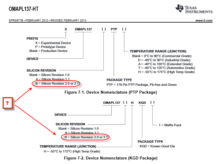
We are working with part # OMAPL137HTBPTPH-YF-1BA1TZW G4, in which the nomenclature on the Datasheet indicates that 'B' indicates silicon version 2.0 or 2.1, can it please be clarified what specific version that is so we can know if the Errata Advisory 2.0.20 is present or not?

This is urgent as we are in the final stages of the bootloader process and we are not sure if we are hitting this bug or not. 

Thanks,

Miguel A. Alanis

  • Update: Can a moderator please move this forum to the OMAPL13x, I don't think I have that capability as a user :).

    Moving this post to the OMAPL Forum as I've verified the si version that I have after running the OMAPL1x_debug.gel file mentioned in one of the boot related wikis, it appears I have Si 2.1, so I should not be facing this bug, however I am still having issues with booting from ARM via SPI1 Flash.

    NEW QUESTION:

    We have modified the CCS Flash writer for our specific SPI Flash however we are having issues after following the instructions on the following wiki. One question that we need help with is are the 'Magic' values required to be placed as we Flash the SPI or is this part of the spi_writer code not required?

    http://processors.wiki.ti.com/index.php/Boot_Images_for_OMAP-L137#Booting_ARM_Binaries

    "---------------------------------------------
    C674X_0: GEL Output: |             Device Information            |
    C674X_0: GEL Output: ---------------------------------------------
    C674X_0: GEL Output: DEV_INFO_00 = 0x9B7DF02F
    C674X_0: GEL Output: DEV_INFO_01 = 0x00000000
    C674X_0: GEL Output: DEV_INFO_02 = 0x0000F376
    C674X_0: GEL Output: DEV_INFO_03 = 0x00000023
    C674X_0: GEL Output: DEV_INFO_04 = 0x00000000
    C674X_0: GEL Output: DEV_INFO_05 = 0x000003E0
    C674X_0: GEL Output: DEV_INFO_06 = 0x80100000
    C674X_0: GEL Output: DEV_INFO_07-DEV_INFO_08-DEV_INFO_09-DEV_INFO_10-DEV_INFO_11-DEV_INFO_12 = 8-0-62763-2-37-34
    C674X_0: GEL Output: DEV_INFO_13,DEV_INFO_14,DEV_INFO_15,DEV_INFO_16 = 1,0,0,12725
    C674X_0: GEL Output: -----
    C674X_0: GEL Output: DEV_INFO_17 = 0x00030003
    C674X_0: GEL Output: DEV_INFO_18 = 0x00000000
    C674X_0: GEL Output: DEV_INFO_19 =C674X_0: GEL Output: 0C674X_0: GEL Output: 0C674X_0: GEL Output: 0C674X_0: GEL Output: 0C674X_0: GEL Output: 0C674X_0: GEL Output:
    C674X_0: GEL Output: -----
    C674X_0: GEL Output: DEV_INFO_20 = 0x30303864
    C674X_0: GEL Output: DEV_INFO_21 = 0x3530306B
    C674X_0: GEL Output: DEV_INFO_22 = 0x00000000
    C674X_0: GEL Output: DEV_INFO_23 = 0x00000000
    C674X_0: GEL Output: -----
    C674X_0: GEL Output: DEV_INFO_24 = 0x02022025
    C674X_0: GEL Output: DEV_INFO_25 = 0x0800F52B
    C674X_0: GEL Output: DEV_INFO_06 = 0x80100000
    C674X_0: GEL Output: DEV_INFO_26 = 0x636A0001
    C674X_0: GEL Output:

    C674X_0: GEL Output: ---------------------------------------------
    C674X_0: GEL Output: |               BOOTROM Info                |
    C674X_0: GEL Output: ---------------------------------------------
    C674X_0: GEL Output: ROM ID: d800k005
    C674X_0: GEL Output: Silicon Revision 2.1
    C674X_0: GEL Output: Boot pins: 62326
    C674X_0: GEL Output: Boot Mode: SPI1 Flash (0x0000F376)
    C674X_0: GEL Output:
    ROM Status Code: 0x00000000
    Description:C674X_0: GEL Output: No error
    C674X_0: GEL Output:
    Program Counter (PC) = 0xA6AA0314
    C674X_0: GEL Output:
    C674X_0: GEL Output: ---------------------------------------------
    C674X_0: GEL Output: |              Clock Information             |
    C674X_0: GEL Output: ---------------------------------------------
    C674X_0: GEL Output:
    C674X_0: GEL Output: PLLs configured to utilize crystal.
    C674X_0: GEL Output: ASYNC3 = PLL0_SYSCLK2
    C674X_0: GEL Output:
    C674X_0: GEL Output: NOTE:  All clock frequencies in following PLL sections are based
    C674X_0: GEL Output: off OSCIN = 24 MHz.  If that value does not match your hardware
    C674X_0: GEL Output: you should change the #define in the top of the gel file, save it,
    C674X_0: GEL Output: and then reload.
    C674X_0: GEL Output:
    C674X_0: GEL Output: ---------------------------------------------
    C674X_0: GEL Output: |              PLL0 Information             |
    C674X_0: GEL Output: ---------------------------------------------
    C674X_0: GEL Output:
    C674X_0: GEL Output: PLL0_SYSCLK1 = 300 MHz
    C674X_0: GEL Output: PLL0_SYSCLK2 = 150 MHz
    C674X_0: GEL Output: PLL0_SYSCLK3 = 100 MHz
    C674X_0: GEL Output: PLL0_SYSCLK4 = 75 MHz
    C674X_0: GEL Output: PLL0_SYSCLK5 = 100 MHz
    C674X_0: GEL Output: PLL0_SYSCLK6 = 300 MHz
    C674X_0: GEL Output: PLL0_SYSCLK7 = 50 MHz
    C674X_0: GEL Output:
    C674X_0: GEL Output: ---------------------------------------------
    C674X_0: GEL Output: |              PSC0 Information             |
    C674X_0: GEL Output: ---------------------------------------------
    C674X_0: GEL Output:
    C674X_0: GEL Output: State Decoder:
    C674X_0: GEL Output:  0 = SwRstDisable (reset asserted, clock off)
    C674X_0: GEL Output:  1 = SyncReset (reset assered, clock on)
    C674X_0: GEL Output:  2 = Disable (reset de-asserted, clock off)
    C674X_0: GEL Output:  3 = Enable (reset de-asserted, clock on)
    C674X_0: GEL Output: >3 = Transition in progress
    C674X_0: GEL Output:
    C674X_0: GEL Output: Module 0:    EDMA3CC (0)        STATE = 0
    C674X_0: GEL Output: Module 1:    EDMA3 TC0          STATE = 0
    C674X_0: GEL Output: Module 2:    EDMA3 TC1          STATE = 0
    C674X_0: GEL Output: Module 3:    EMIFA (BR7)        STATE = 3
    C674X_0: GEL Output: Module 4:    SPI 0              STATE = 0
    C674X_0: GEL Output: Module 5:    MMC/SD 0           STATE = 0
    C674X_0: GEL Output: Module 6:    AINTC              STATE = 3
    C674X_0: GEL Output: Module 7:    ARM RAM/ROM        STATE = 3
    C674X_0: GEL Output: Module 9:    UART 0             STATE = 0
    C674X_0: GEL Output: Module 10:    SCR 0 (BR0/1/2/8)  STATE = 3
    C674X_0: GEL Output: Module 11:    SCR 1 (BR4)        STATE = 3
    C674X_0: GEL Output: Module 12:    SCR 2 (BR3/5/6)    STATE = 3
    C674X_0: GEL Output: Module 13:    PRUSS              STATE = 0
    C674X_0: GEL Output: Module 14:    ARM                STATE = 0
    C674X_0: GEL Output: Module 15:    DSP                STATE = 3
    C674X_0: GEL Output:
    C674X_0: GEL Output: ---------------------------------------------
    C674X_0: GEL Output: |              PSC1 Information             |
    C674X_0: GEL Output: ---------------------------------------------
    C674X_0: GEL Output:
    C674X_0: GEL Output: State Decoder:
    C674X_0: GEL Output:  0 = SwRstDisable (reset asserted, clock off)
    C674X_0: GEL Output:  1 = SyncReset (reset assered, clock on)
    C674X_0: GEL Output:  2 = Disable (reset de-asserted, clock off)
    C674X_0: GEL Output:  3 = Enable (reset de-asserted, clock on)
    C674X_0: GEL Output: >3 = Transition in progress
    C674X_0: GEL Output:
    C674X_0: GEL Output: Module 1:    USB0 (2.0)         STATE = 0
    C674X_0: GEL Output: Module 2:    USB1 (1.1)         STATE = 0
    C674X_0: GEL Output: Module 3:    GPIO               STATE = 0
    C674X_0: GEL Output: Module 4:    UHPI               STATE = 0
    C674X_0: GEL Output: Module 5:    EMAC               STATE = 0
    C674X_0: GEL Output: Module 6:    EMIFB (BR20)       STATE = 3
    C674X_0: GEL Output: Module 7:    MCASP0 + FIFO      STATE = 0
    C674X_0: GEL Output: Module 8:    MCASP1 + FIFO      STATE = 0
    C674X_0: GEL Output: Module 9:    MCASP2 + FIFO      STATE = 0
    C674X_0: GEL Output: Module 10:    SPI 1              STATE = 3
    C674X_0: GEL Output: Module 11:    I2C 1              STATE = 0
    C674X_0: GEL Output: Module 12:    UART 1             STATE = 0
    C674X_0: GEL Output: Module 13:    UART 2             STATE = 0
    C674X_0: GEL Output: Module 16:    LCDC               STATE = 0
    C674X_0: GEL Output: Module 17:    eHRPWM (all)       STATE = 0
    C674X_0: GEL Output: Module 20:    eCAP (all)         STATE = 0
    C674X_0: GEL Output: Module 21:    eQEP 0/1           STATE = 0
    C674X_0: GEL Output: Module 24:    SCR8 (Br15)        STATE = 3
    C674X_0: GEL Output: Module 25:    SCR7 (Br12)        STATE = 3
    C674X_0: GEL Output: Module 26:    SCR12 (Br18)       STATE = 3
    C674X_0: GEL Output: Module 31:    L3 RAM (Br13)      STATE = 3

    "

    Regards,

    Miguel

  • Hi Miguel,

    For OMAP-L137, as you might already know that there are two methods available to flash images to SPI.

    1. One is serial flasher utility ( only for pre-built UBL) http://processors.wiki.ti.com/index.php/Serial_Boot_and_Flash_Loading_Utility_for_OMAP-L137 and the other is

    2. CCS (SPI/NAND) flash writer.

    You have chosen the second option, CCS SPI flash writer. After modifying it, were you able to flash the images successfully? Did you burn all these files:- DSP AIS, ARM UBL and U-Boot?

    I would like to understand at which stage you experienced problem? whether during flashing into SPI or booting from SPI after flashing?

    If you are able to flash the images successfully, what are all the images you flashed? whether these images are pre-built or Custom? Did you generate a single AIS image? using hexgentool? While creating a single AIS image, the order of the source .out files is important as the boot loader will jump to the entrypoint of the first .out file listed, which in this case is the DSP UBL ( as the OMAPL137 is the DSP boot device; which means DSP wakes up first which in turn wake up the ARM)

    In your case, it definitely requires the DSP UBL and ARM application program which in turn to be merged as a single AIS image using Hexgentool provided that the order of the binary files to be the first binary of DSP UBL and then the binary of ARM application.

    I think, the magic values need not to be changed.

    Some useful TI wiki links:

    Flashing images to SPI:

    http://processors.wiki.ti.com/index.php/GSG:_DA8x/OMAP-L1/AM1x_DVEVM_Additional_Procedures#Flashing_images_to_SPI_Flash_2

    Generating ARM AIS File for OMAP-L137:-

    http://processors.wiki.ti.com/index.php/GSG:_Building_Software_Components_for_OMAP-L1#For_OMAP-L137_.28or_DA830.2C_AM17xx.29

    Rebuilding the SPI flash writer:

    http://processors.wiki.ti.com/index.php/GSG:_Building_Software_Components_for_OMAP-L1#Rebuilding_the_SPI_Flash_writer

    Regards,

    Shankari.

    -------------------------------------------------------------------------------------------------------

    Please click the Verify Answer button on this post if it answers your question.
    -------------------------------------------------------------------------------------------------------- 

  • updated post with a picture showing the confusion point in the OMAPL137HT datasheet.-M.Alanis

    Shankari

    Thanks for the valuable information and links, it would have been helpful to have them all in one common place though (like the bootloader appnote). It was painfull to go through so many bits and pieces of good information scattered in several places (bootloader appnote + wikis etc+dsheet+peripheral userguide) .

    I have resolved my issue and am able to successfully flash my code using the spi flash writer (modified for my custom SPI).

    Starting with the bootloader appnote: http://www.ti.com/lit/an/sprab04g/sprab04g.pdf

    then http://processors.wiki.ti.com/index.php/Boot_Images_for_OMAP-L137#Booting_ARM_Binaries

    Then get and modify TI's sample CCS code for DSP+ARM Booting: http://processors.wiki.ti.com/images/8/85/OMAPL137-ARM-LED-v1.zip

    Then modifying the linker command file sample code (DSP Boot side, to place DSP UBL(Boot code) away from SHARED RAM and into a L memory to avoid not being overwritten by the ARM UBL)  BTW this needs to be emphasized a lot more as we has all of our ARM UBL in SHARED RAM and overwrote it causing the DSP to go into the weeds and caused painful debug.

    This is the Bootloader Debug gel file http://processors.wiki.ti.com/index.php/OMAP-L1x_Debug_Gel_Files to be able to distinguish which Version of the silicon 2.0 or 2.1, a note on the nomenclature would have helped.

    update: of confusion area that needs clarification on the OMAPL137HT datasheet or instruct a way on how to determine this.

    and followed by the helpful links above.

    Thanks,

    Miguel A. Alanis

  • Hi Miguel,

    Would you please reload the picture? Might be some problem during attachment.


    Regards,

    Shankari

  • Hi MAlanis,

    Running the OMAPL1x_debug.gel will determine the silicon revision and I believe it as a correct method.


    Regards,

    Shankari