This thread has been locked.

If you have a related question, please click the "Ask a related question" button in the top right corner. The newly created question will be automatically linked to this question.

Query related to DSP TMS320C6746 internal memory

Other Parts Discussed in Thread: TMS320C6746

4544.tms320c6746.pdfHere we are using HPI of TMS320C6746. 1) What is the start and end address range of internal memory FOrHPI communication. Can I use whole 0x0000 0000 to 0xFFFF FFFF for HPI communication.? 2) Open attached pdf page no. 21, In that address range 0x0080 0000 to 0x0083 FFFF is for DSP L2 RAM. And on Page no.23 In that address range 0x1180 0000 0x1183 FFFF is also for DSP L2 RAM. Whats the difference between this two.? Both are L2 RAM but having different address ranges.

  • Rahul Shah,

    If any sections of the DSP memory map are located in DSP L2 RAM (0x11800000), be aware of two things: 

    1. Make sure all L2 RAM addresses in the DSP linker command file are referenced in the 0x118xxxxx range and not 0x008xxxxx, as the ARM(If OMAP-L13x device) cannot write to the 0x008xxxxx address range 
    2. Use the "Configure PSC" function of AISGen to enable the DSP LPSC (PSC0,#15). If the DSP megamodule is in reset, the L2 RAM will not be accessible so the section loads will fail.

    0x0080 0000 0x0083 FFFF - 256K DSP L2 RAM
    0x1180 0000 0x1183 FFFF - 256K DSP L2 RAM

    The memMap configuration parameter defines the on-chip memory map for the device. Define the amount of L2 RAM used for L2 Cache.


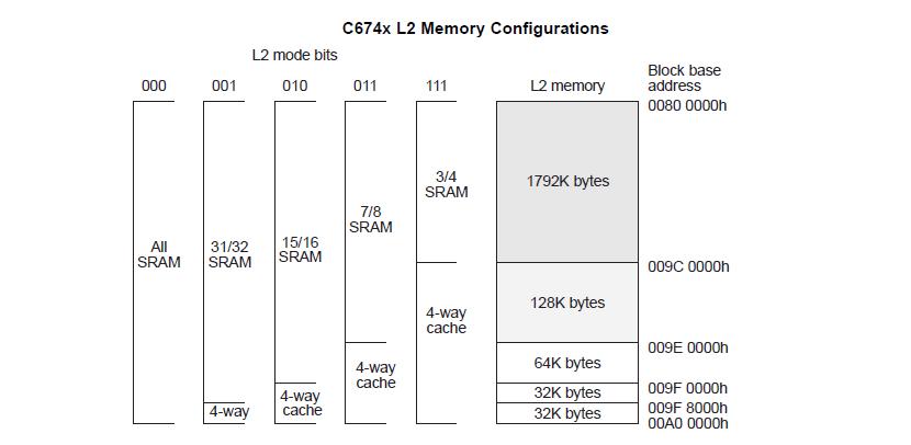
    Level 2 memory (L2) can also be split into L2 RAM (normal addressable on-chip memory) and L2 cache for caching external memory locations. It is one of the internal memories of the DSP subsystem.

    L2 memory includes 256 KB of RAM. The DSP unified memory controller (UMC) allows you to configure part or all of the L2 RAM as normal RAM or as cache. You can configure cache sizes of 0 KB, 4 KB, 8 KB, 16 KB, 32 KB, 64 KB, 128 KB, or 256 KB of the 256 KB of RAM. The default configuration is 256 KB normal RAM.

    L2 memory can be configured as mapped memory, cache, or combinations of the two.

    Please refer this thread for HPI, this will help you.
    http://e2e.ti.com/support/dsp/tms320c6000_high_performance_dsps/f/112/t/34534.aspx

  • Hi

    As Pubesh mentioned, 0x11 8 xyz starting address for the L2 is the same physical memory as 0x00 8xyz , it is just that any external to DSP masters (like HPI, EDMA etc) use 0x11 8xyz as the address (global address) , which is internally decoded by the DSP as accesses to its L2.

    You can see the same info in the memory map view in the datasheet.

    For ease of use and all practical purposes, you can use the global address across, the board in your linker command files etc.

    Please also see the following post on additional restrictions on which memory maps are not accessible over HPI

    https://e2e.ti.com/support/dsp/omap_applications_processors/int_omapl1x_dsps/f/116/p/12597/49384.aspx#49384

    The above post is for 6747 , but also applies to c6746.

    Regards

    Mukul

  • Hi Mukul and Pubesh,

    Thanks for yor reply.

    I read ,and i conclude that,

    1) If i have to use 256KB L2 RAM for HPI,then master host have to write in address range 0x1180 0000 0x1183 FFFF.

    2) And our CPU DSP deode that from that address range ,Means address range 0x1180 0000 0x1183 FFFF

    are internally mapped with  0x0080 0000 to 0x0083 FFFF?

    3) Host master cant write in  0x0080 0000 to 0x0083 FFFF?

    4) What is the start and end address range of internal memory which can i use for HPI communication?

    5)Can I use whole 0x0000 0000 to 0xFFFF FFFF for HPI communication.?

    Regards,

    Rahul Shah

  • Hi Rahul

    On 4 and 5, I recommend looking at the boot loader application note for any restriction on L2/Shared Ram memory during HPI boot, and for overall accessibility range you can refer to the datasheet Table 2-4, the last column is the "Master peripheral Memory Map" , and UHPI is one of the bus masters, so the ranges shown accessible for that column apply to UHPI also.

    Just keep in mind as I mentioned in my previous post, UHPI cannot access the SYSCFG registers as several of those registers require privilege mode access that is only possible by DSP.

    Regards

    Mukul

  • Hi mukul,

     And what's about topic 1,2, & 3.

    Regards,

    Rahul Shah

  • Yes your understanding on 1,2 & 3 is correct.

    Regards

    Mukul