This thread has been locked.

If you have a related question, please click the "Ask a related question" button in the top right corner. The newly created question will be automatically linked to this question.

[Urgent] Confirm the XF pin behavior

Guru 24520 points

Hi,

Please let me confirm the following questions.

1.  What kinds of XF pin status is assumed when perform the reset to C5535/C5515 or the POWERGOOD signal is "Low"?

i.e. I would like to know whether XF pin will be unstable(X).

2. If assumed that XF pin will be both status "H" and  "L",  is it potential that the XF pin behavior will change by the timing of dropping the voltage VDD_PLL and DSP_LDO?

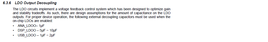
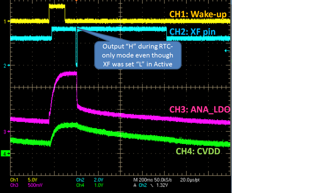
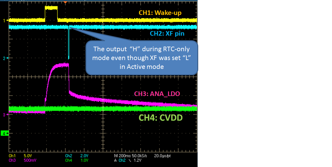
According to the customer's board, if the DSP_LDO powered down after the VDD_PLL(i.e. Change the status from active to RTC only mode), XF pin was generated the "H" even though the S/W did not set the register of XF.  In addition to this, If the DSP_LDO will power down before the VDD_PLL, this phenomenon did not confirm.

I attached this waveform as below. 

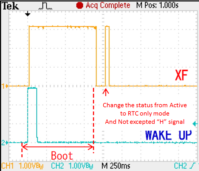
Sometimes, this "H" signal did not appear on XF pin.

If you have any questions, please let me know.

Best regards.

Kaka

  • Kaka-san,

    XF is unstable when POWERGOOD is low and goes to "1" afterward. This is clearly stated in Pin Behavior at Reset.

    As for the power sequence, it is not specified. XF is onfigured by a bit in DSP core. By power down the core first before the clock would be more logical.

    I will be traveling and will not haveaccess to computer.

    Regards.

  • HI Steve,


    Thank you for your response.  I understood that XF is unstable when POWERGOOD is low and goes to "High" afterward.

     > By power down the core first before the clock would be more logical.

    How should we control the power sequence which you wrote in previous post  in case of using internal LDOs?

    I think that the internal LDOs were disabled at a time by register(BG_PD/LDO_PD)  when goes to RTC only mode.  As a result, we can not control the timing of the voltage of  VDD_PLL and CVDD by using internal LDOs.

    In addition to this, regarding to the datasheet, the LDO output decoupling was as below.

    This inform to us that power-down the clock first before the core. It seems that this description was against your opinion.

    Also please provide your advice to us for XF pin behavior.

    In our evaluation, when there are few voltage on CVDD before power-down the VDD_PLL, the XF was outputted High even though XF was configured "0" in DSP register before goes to RTC-only mode.

    Note: In order to confirm this phenomenon, I added a capacitor(100uF) to CVDD line in order to have some voltage after power-down the DSP_LDO.  Please see the waveform as below

    [Question]

    I can not understand why this phenomenon was happened.  Would you please explain the logical?

    If you have any questions, please let me know.

    Best regards.

    Kaka

  • Hi Steve,

    I have question/Request in addition to my previous post.

    The core will work until the supply voltage to core will be under  0.998mV. So, the core can work a few mili second after entering the RTC-only mode.  At this time, the C55x will be in "while loop" as below.

    --------------------------------------------

            while (1)
            {
                    temp1920 = *(volatile ioport unsigned int *) (0x1920);
                    if ((temp1920&0x0020)!=0)
                    {
                    asm(" *port(#0x1920) = #0x803F "); //clear interrupt flags
                    asm(" *port(#0x1930) = #0x0006 "); //WU_DIR input & LDO & BG shutdown
                    asm(" *port(#0x1920) = #0x803F "); //clear interrupt flags
                    }
    }

    --------------------------------------------

    Regarding to the datasheet, the supply voltage of CVDD is designed to be supplied longer than VDDA_PLL by capacitance.  So, there is a situation that the CVDD works and VDDA_PLL is disabled. In this situation, the PLL of C55x will be bypass mode during RTC only mode. So, if the VDDA_PLL is disabled when CVDD is powered, there are not any influence for the operation of device. However, we got unintended operation as below waveforms.

    Note: The following waveform is that continue to supply the power to CVDD in RTC-only mode by using C5515EVM.

    [Question]

    Any idea how this happened?

    In addition to this question, I have one request to you.

    [Request]
    According to our observation, if power down the core first before PLL, there is not any influence for the operation.  However, we did not have no evidence to do this workaround. 

    So would you please explain the reason in logical?

    If you have any question, please let me know.

    Best regards.

    Kaka

  • Kaka-san

    Steve and most of the c55x apps is now on vacation. We will need to get back to you on this after 6th Jan. This will likely need some analysis in the lab once the team is back.

    We will keep you posted.

    Regards

    Mukul

  • Hi Mukul,

    Thank you for you supports.

    The priority of this topics is higher than other my posts such as "Appear the unintended voltage on ANA_LDO" or "Bus holder behavior".  So, if possible, would you please correspond this topics with high priority?


    Best regards,

    Kaka