


Other Parts Discussed in Thread: OMAPL138, CCSTUDIO
I'm trying to get my code build setup so that I can do program my 6748 SOM for stand-alone operation. I used the GEL file for the C6748 that seems to work fine when I'm running things from the debugger to create initialization code. The problem is this: I call the function Set_mDDR_132MHz() (which in turn calls the functions device_PLL1 and DEVICE_mDDRConfig). I build this as a debug build with no optimizations. I load the code from the debugger and then run it from the debugger. The 6748 hangs. When I try to do a manual break (Shift-F5), I get the following message from CC Studio:
"CPU pipeline is stalled and the CPU is 'not ready'. This means
that the CPU has performed an access which has not
completed, and the CPU is waiting."
There's also all the extra verbage about disconnecting the target and restarting, etc. etc.
Anyway, below is the config code I'm using:
#define PLL0_BASE 0x01C11000 //SYSTEM PLL BASE ADDRESS
#define PLL0_PID *(unsigned int*) (PLL0_BASE + 0x00) //PID
#define PLL0_FUSERR *(unsigned int*) (PLL0_BASE + 0xE0) //x*FuseFarm Error Reg
#define PLL0_RSTYPE *(unsigned int*) (PLL0_BASE + 0xE4) //Reset Type status Reg
#define PLL0_PLLCTL *(unsigned int*) (PLL0_BASE + 0x100) //PLL Control Register
#define PLL0_OCSEL *(unsigned int*) (PLL0_BASE + 0x104) //OBSCLK Select Register
#define PLL0_SECCTL *(unsigned int*) (PLL0_BASE + 0x108) //PLL Secondary Control Register
#define PLL0_PLLM *(unsigned int*) (PLL0_BASE + 0x110) //PLL Multiplier
#define PLL0_PREDIV *(unsigned int*) (PLL0_BASE + 0x114) //Pre divider
#define PLL0_PLLDIV1 *(unsigned int*) (PLL0_BASE + 0x118) //Divider-1
#define PLL0_PLLDIV2 *(unsigned int*) (PLL0_BASE + 0x11C) //Divider-2
#define PLL0_PLLDIV3 *(unsigned int*) (PLL0_BASE + 0x120) //Divider-3
#define PLL0_OSCDIV1 *(unsigned int*) (PLL0_BASE + 0x124) //Oscilator Divider
#define PLL0_POSTDIV *(unsigned int*) (PLL0_BASE + 0x128) //Post Divider
#define PLL0_BPDIV *(unsigned int*) (PLL0_BASE + 0x12C) //Bypass Divider
#define PLL0_WAKEUP *(unsigned int*) (PLL0_BASE + 0x130) //Wakeup Reg
#define PLL0_PLLCMD *(unsigned int*) (PLL0_BASE + 0x138) //Command Reg
#define PLL0_PLLSTAT *(unsigned int*) (PLL0_BASE + 0x13C) //Status Reg
#define PLL0_ALNCTL *(unsigned int*) (PLL0_BASE + 0x140) //Clock Align Control Reg
#define PLL0_DCHANGE *(unsigned int*) (PLL0_BASE + 0x144) //PLLDIV Ratio Chnage status
#define PLL0_CKEN *(unsigned int*) (PLL0_BASE + 0x148) //Clock Enable Reg
#define PLL0_CKSTAT *(unsigned int*) (PLL0_BASE + 0x14C) //Clock Status Reg
#define PLL0_SYSTAT *(unsigned int*) (PLL0_BASE + 0x150) //Sysclk status reg
#define PLL0_PLLDIV4 *(unsigned int*) (PLL0_BASE + 0x160) //Divider 4
#define PLL0_PLLDIV5 *(unsigned int*) (PLL0_BASE + 0x164) //Divider 5
#define PLL0_PLLDIV6 *(unsigned int*) (PLL0_BASE + 0x168) //Divider 6
#define PLL0_PLLDIV7 *(unsigned int*) (PLL0_BASE + 0x16C) //Divider 7
#define PLL0_PLLDIV8 *(unsigned int*) (PLL0_BASE + 0x170) //Divider 8
#define PLL0_PLLDIV9 *(unsigned int*) (PLL0_BASE + 0x174) //Divider 9
#define PLL0_PLLDIV10 *(unsigned int*) (PLL0_BASE + 0x178) //Divider 10
#define PLL0_PLLDIV11 *(unsigned int*) (PLL0_BASE + 0x17C) //Divider 11
#define PLL0_PLLDIV12 *(unsigned int*) (PLL0_BASE + 0x180) //Divider 12
#define PLL0_PLLDIV13 *(unsigned int*) (PLL0_BASE + 0x184) //Divider 13
#define PLL0_PLLDIV14 *(unsigned int*) (PLL0_BASE + 0x188) //Divider 14
#define PLL0_PLLDIV15 *(unsigned int*) (PLL0_BASE + 0x18C) //Divider 15
#define PLL0_PLLDIV16 *(unsigned int*) (PLL0_BASE + 0x190) //Divider 16
#define PLL1_BASE 0x01E1A000 //SYSTEM PLL1 BASE ADDRESS
#define PLL1_PID *(unsigned int*) (PLL1_BASE + 0x00) //PID
#define PLL1_FUSERR *(unsigned int*) (PLL1_BASE + 0xE0) //x*FuseFarm Error Reg
#define PLL1_RSTYPE *(unsigned int*) (PLL1_BASE + 0xE4) //Reset Type status Reg
#define PLL1_PLLCTL *(unsigned int*) (PLL1_BASE + 0x100) //PLL Control Register
#define PLL1_OCSEL *(unsigned int*) (PLL1_BASE + 0x104) //OBSCLK Select Register
#define PLL1_SECCTL *(unsigned int*) (PLL1_BASE + 0x108) //PLL Secondary Control Register
#define PLL1_PLLM *(unsigned int*) (PLL1_BASE + 0x110) //PLL Multiplier
#define PLL1_PREDIV *(unsigned int*) (PLL1_BASE + 0x114) //Pre divider
#define PLL1_PLLDIV1 *(unsigned int*) (PLL1_BASE + 0x118) //Divider-1
#define PLL1_PLLDIV2 *(unsigned int*) (PLL1_BASE + 0x11C) //Divider-2
#define PLL1_PLLDIV3 *(unsigned int*) (PLL1_BASE + 0x120) //Divider-3
#define PLL1_OSCDIV1 *(unsigned int*) (PLL1_BASE + 0x124) //Oscilator Divider
#define PLL1_POSTDIV *(unsigned int*) (PLL1_BASE + 0x128) //Post Divider
#define PLL1_BPDIV *(unsigned int*) (PLL1_BASE + 0x12C) //Bypass Divider
#define PLL1_WAKEUP *(unsigned int*) (PLL1_BASE + 0x130) //Wakeup Reg
#define PLL1_PLLCMD *(unsigned int*) (PLL1_BASE + 0x138) //Command Reg
#define PLL1_PLLSTAT *(unsigned int*) (PLL1_BASE + 0x13C) //Status Reg
#define PLL1_ALNCTL *(unsigned int*) (PLL1_BASE + 0x140) //Clock Align Control Reg
#define PLL1_DCHANGE *(unsigned int*) (PLL1_BASE + 0x144) //PLLDIV Ratio Chnage status
#define PLL1_CKEN *(unsigned int*) (PLL1_BASE + 0x148) //Clock Enable Reg
#define PLL1_CKSTAT *(unsigned int*) (PLL1_BASE + 0x14C) //Clock Status Reg
#define PLL1_SYSTAT *(unsigned int*) (PLL1_BASE + 0x150) //Sysclk status reg
#define PLL1_PLLDIV4 *(unsigned int*) (PLL1_BASE + 0x160) //Divider 4
#define PLL1_PLLDIV5 *(unsigned int*) (PLL1_BASE + 0x164) //Divider 5
#define PLL1_PLLDIV6 *(unsigned int*) (PLL1_BASE + 0x168) //Divider 6
#define PLL1_PLLDIV7 *(unsigned int*) (PLL1_BASE + 0x16C) //Divider 7
#define PLL1_PLLDIV8 *(unsigned int*) (PLL1_BASE + 0x170) //Divider 8
#define PLL1_PLLDIV9 *(unsigned int*) (PLL1_BASE + 0x174) //Divider 9
#define PLL1_PLLDIV10 *(unsigned int*) (PLL1_BASE + 0x178) //Divider 10
#define PLL1_PLLDIV11 *(unsigned int*) (PLL1_BASE + 0x17C) //Divider 11
#define PLL1_PLLDIV12 *(unsigned int*) (PLL1_BASE + 0x180) //Divider 12
#define PLL1_PLLDIV13 *(unsigned int*) (PLL1_BASE + 0x184) //Divider 13
#define PLL1_PLLDIV14 *(unsigned int*) (PLL1_BASE + 0x188) //Divider 14
#define PLL1_PLLDIV15 *(unsigned int*) (PLL1_BASE + 0x18C) //Divider 15
#define PLL1_PLLDIV16 *(unsigned int*) (PLL1_BASE + 0x190) //Divider 16
//PSC Module Related Registers
#define PSC0_BASE 0x01C10000
#define PSC1_BASE 0x01E27000
#define PSC0_MDCTL (PSC0_BASE+0xA00)
#define PSC0_MDSTAT (PSC0_BASE+0x800)
#define PSC0_PTCMD *(unsigned int*) (PSC0_BASE + 0x120)
#define PSC0_PTSTAT *(unsigned int*) (PSC0_BASE + 0x128)
#define PSC1_MDCTL (PSC1_BASE+0xA00)
#define PSC1_MDSTAT (PSC1_BASE+0x800)
#define PSC1_PTCMD *(unsigned int*) (PSC1_BASE + 0x120)
#define PSC1_PTSTAT *(unsigned int*) (PSC1_BASE + 0x128)
#define LPSC_EDMA_CC0 0
#define LPSC_EDMA_TC0 1
#define LPSC_EDMA_TC1 2
#define LPSC_EMIFA 3 //PSC0
#define LPSC_SPI0 4 //PSC0
#define LPSC_MMCSD0 5 //PSC0
#define LPSC_ARM_AINTC 6
#define LPSC_ARM_RAMROM 7 //PSC0
// LPSC #8 not used
#define LPSC_UART0 9 //PSC0
#define LPSC_SCR0 10
#define LPSC_SCR1 11
#define LPSC_SCR2 12
// LPSC #13 not used
#define LPSC_ARM 14 //PSC0
#define LPSC_DSP 15 //PSC0
#define LPSC_EDMA_CC1 0
#define LPSC_USB20 1 //PSC1
#define LPSC_USB11 2 //PSC1
#define LPSC_GPIO 3 //PSC1
#define LPSC_UHPI 4 //PSC1
#define LPSC_EMAC 5 //PSC1
#define LPSC_DDR 6 //PSC1
#define LPSC_MCASP0 7 //PSC1
#define LPSC_SATA 8 //PSC1
#define LPSC_VPIF 9 //PSC1
#define LPSC_SPI1 10 //PSC1
#define LPSC_I2C1 11 //PSC1
#define LPSC_UART1 12 //PSC1
#define LPSC_UART2 13 //PSC1
#define LPSC_MCBSP0 14 //PSC1
#define LPSC_MCBSP1 15 //PSC1
#define LPSC_LCDC 16 //PSC1
#define LPSC_EPWM 17 //PSC1
#define LPSC_MMCSD1 18
#define LPSC_UPP 19
#define LPSC_ECAP 20
#define LPSC_EDMA_TC2 21
// LPSC #22-23 not used
#define LPSC_SCR_F0 24
#define LPSC_SCR_F1 25
#define LPSC_SCR_F2 26
#define LPSC_SCR_F6 27
#define LPSC_SCR_F7 28
#define LPSC_SCR_F8 29
#define LPSC_BR_F7 30
#define LPSC_SHARED_RAM 31
//DDR MMR Declaration
#define EMIF3A_SDRAM_CFG 0xB0000000
#define VTPIO_CTL *(unsigned int*)(0x01E2C000) // VTPIO_CTL Register
#define EMIF3A_REVID *(unsigned int*)(EMIF3A_SDRAM_CFG + 0x00) //EMIF Module ID and Revision Register
#define EMIF3A_SDRSTAT *(unsigned int*)(EMIF3A_SDRAM_CFG + 0x04) //SDRAM Status Register
#define EMIF3A_SDCR *(unsigned int*)(EMIF3A_SDRAM_CFG + 0x08) //SDRAM Bank Config Register
#define EMIF3A_SDRCR *(unsigned int*)(EMIF3A_SDRAM_CFG + 0x0C) //SDRAM Refresh Control Register
#define EMIF3A_SDTIMR1 *(unsigned int*)(EMIF3A_SDRAM_CFG + 0x10) //SDRAM Timing Register1
#define EMIF3A_SDTIMR2 *(unsigned int*)(EMIF3A_SDRAM_CFG + 0x14) //SDRAM Timing Register2
#define EMIF3A_SDCR2 *(unsigned int*)(EMIF3A_SDRAM_CFG + 0x1C) //SDRAM Config Register2
#define EMIF3A_PBBPR *(unsigned int*)(EMIF3A_SDRAM_CFG + 0x20) //VBUSM Burst Priority Register
#define EMIF3A_VBUSMCFG1 *(unsigned int*)(EMIF3A_SDRAM_CFG + 0x28) //VBUSM config Value1 Register
#define EMIF3A_VBUSMCFG2 *(unsigned int*)(EMIF3A_SDRAM_CFG + 0x2C) //VBUSM config Value2 Register
#define EMIF3A_IRR *(unsigned int*)(EMIF3A_SDRAM_CFG + 0xC0) //Interrupt Raw Register
#define EMIF3A_IMR *(unsigned int*)(EMIF3A_SDRAM_CFG + 0xC4) //Interrupt Masked Register
#define EMIF3A_IMSR *(unsigned int*)(EMIF3A_SDRAM_CFG + 0xC8) //Interrupt Mask Set Register
#define EMIF3A_IMCR *(unsigned int*)(EMIF3A_SDRAM_CFG + 0xCC) //Interrupt Mask Clear Register
#define DDRPHYREV *(unsigned int*)(EMIF3A_SDRAM_CFG + 0xE0) //DDR PHY ID and Revision Register
#define DDRCTL *(unsigned int*)(EMIF3A_SDRAM_CFG + 0xE4) //DDR PHY Control 1 Register
#define DDRPHYCTL2 *(unsigned int*)(EMIF3A_SDRAM_CFG + 0xE8) //DDR PHY Control 2 Register
#define EMIF3A_BASE_ADDR 0xC0000000
#define EMIF25_BASE_ADDR 0x40000000
#define EMIF25_CS2_BASE_ADDR 0x60000000
#define EMIF25_CS3_BASE_ADDR 0x62000000
#define EMIF25_CS4_BASE_ADDR 0x64000000
#define EMIF25_CS5_BASE_ADDR 0x66000000
//EMIF2.5 MMR Declaration
#define EMIF25 0x68000000
#define EMIF25_AWAITCFG *(unsigned int*)(EMIF25 + 0x04)
#define EMIF25_SDCFG *(unsigned int*)(EMIF25 + 0x08)
#define EMIF25_SDREF *(unsigned int*)(EMIF25 + 0x0C)
#define EMIF25_ACFG2 *(unsigned int*)(EMIF25 + 0x10) //Async Bank1 Config Register
#define EMIF25_ACFG3 *(unsigned int*)(EMIF25 + 0x14) //Async Bank2 Config Register
#define EMIF25_ACFG4 *(unsigned int*)(EMIF25 + 0x18) //Async Bank3 Config Register
#define EMIF25_ACFG5 *(unsigned int*)(EMIF25 + 0x1C) //Async Bank4 Config Register
#define EMIF25_SDTIM *(unsigned int*)(EMIF25 + 0x20) //SDRAM Timing Register
#define EMIF25_SRPD *(unsigned int*)(EMIF25 + 0x3C)
#define EMIF25_NANDFCR *(unsigned int*)(EMIF25 + 0x60)
//GPIO MMR
#define GPIO_REG_BASE (0x01E26000)
#define GPIO_BANK_OFFSET (0x28)
#define GPIO_DAT_OFFSET (0x04)
#define GPIO_SET_OFFSET (0x08)
#define GPIO_CLR_OFFSET (0x0C)
#define GPIO_BINTEN *(unsigned int*)(GPIO_REG_BASE + 0x08)
#define GPIO_BANK01_BASE (GPIO_REG_BASE + 0x10)
#define GPIO_BANK23_BASE (GPIO_BANK01_BASE + GPIO_BANK_OFFSET)
#define GPIO_BANK45_BASE (GPIO_BANK23_BASE + GPIO_BANK_OFFSET)
#define GPIO_BANK67_BASE (GPIO_BANK45_BASE + GPIO_BANK_OFFSET)
#define GPIO_BANK8_BASE (GPIO_BANK67_BASE + GPIO_BANK_OFFSET)
#define GPIO_BANK23_DIR *(unsigned int*)(GPIO_BANK23_BASE)
#define GPIO_BANK23_DAT *(unsigned int*)(GPIO_BANK23_BASE + GPIO_DAT_OFFSET)
#define GPIO_BANK23_SET *(unsigned int*)(GPIO_BANK23_BASE + GPIO_SET_OFFSET)
#define GPIO_BANK23_CLR *(unsigned int*)(GPIO_BANK23_BASE + GPIO_CLR_OFFSET)
//System MMR Declaration
#define SYS_BASE 0x01C14000
#define HOST0CFG *(unsigned int*)(SYS_BASE + 0x040) //ARM HOST0CFG
#define KICK0R *(unsigned int*)(SYS_BASE + 0x038)
#define KICK1R *(unsigned int*)(SYS_BASE + 0x03c)
#define PINMUX0 *(unsigned int*)(SYS_BASE + 0x120) //PINMUX0
#define PINMUX1 *(unsigned int*)(SYS_BASE + 0x124) //PINMUX1
#define PINMUX2 *(unsigned int*)(SYS_BASE + 0x128) //PINMUX2
#define PINMUX3 *(unsigned int*)(SYS_BASE + 0x12C) //PINMUX3
#define PINMUX4 *(unsigned int*)(SYS_BASE + 0x130) //PINMUX4
#define PINMUX5 *(unsigned int*)(SYS_BASE + 0x134) //PINMUX5
#define PINMUX6 *(unsigned int*)(SYS_BASE + 0x138) //PINMUX6
#define PINMUX7 *(unsigned int*)(SYS_BASE + 0x13C) //PINMUX7
#define PINMUX8 *(unsigned int*)(SYS_BASE + 0x140) //PINMUX8
#define PINMUX9 *(unsigned int*)(SYS_BASE + 0x144) //PINMUX9
#define PINMUX10 *(unsigned int*)(SYS_BASE + 0x148) //PINMUX10
#define PINMUX11 *(unsigned int*)(SYS_BASE + 0x14C) //PINMUX11
#define PINMUX12 *(unsigned int*)(SYS_BASE + 0x150) //PINMUX12
#define PINMUX13 *(unsigned int*)(SYS_BASE + 0x154) //PINMUX13
#define PINMUX14 *(unsigned int*)(SYS_BASE + 0x158) //PINMUX14
#define PINMUX15 *(unsigned int*)(SYS_BASE + 0x15C) //PINMUX15
#define PINMUX16 *(unsigned int*)(SYS_BASE + 0x160) //PINMUX16
#define PINMUX17 *(unsigned int*)(SYS_BASE + 0x164) //PINMUX17
#define PINMUX18 *(unsigned int*)(SYS_BASE + 0x168) //PINMUX18
#define PINMUX19 *(unsigned int*)(SYS_BASE + 0x16C) //PINMUX19
#define CFGCHIP0 *(unsigned int*)(SYS_BASE + 0x17C)
#define CFGCHIP2 *(unsigned int*)(SYS_BASE + 0x184)
#define CFGCHIP3 *(unsigned int*)(SYS_BASE + 0x188)
#define PD0 0 //Power Domain-0
#define PD1 1 //Power Domain-1
#define PLLEN_MUX_SWITCH 4
#define PLL_LOCK_TIME_CNT 2400
#define PLL_STABILIZATION_TIME 2000
#define PLL_RESET_TIME_CNT 200
/*// ------------------------------------------------------------------------
//
// Setup_System_Config( )
// Configure PINMUX and other system module registers
//
// ------------------------------------------------------------------------ //
void Setup_System_Config(void)
{
KICK0R = 0x83e70b13; // Kick0 register + data (unlock)
KICK1R = 0x95a4f1e0; // Kick1 register + data (unlock)
PINMUX0 = 0x11111188; // EMIFB, Check EMU0/RTCK
PINMUX1 = 0x11111111; // EMIFB
PINMUX2 = 0x11111111; // EMIFB
PINMUX3 = 0x11111111; // EMIFB
PINMUX4 = 0x11111111; // EMIFB
PINMUX5 = 0x11111111; // EMIFB
PINMUX6 = 0x11111111; // EMIFB
PINMUX7 = 0x11111111; // EMIFB, SPI0
PINMUX8 = 0x21122111; // UART2, McASP1, I2C0, I2C1
PINMUX9 = 0x11011112; // RMII CLK, McASP0, USB_DRVVBUS, UART2
PINMUX10 = 0x22222221; // RMII/ McASP0
//PINMUX11 = 0x11112222; // McASP1, UART1, McASP0, MDIO (last 2 digits 0x22 for MDIO instead of GPIO)
PINMUX11 = 0x00001100; //Enable Uart1 by default - Thomas Price
PINMUX12 = 0x11111111; // McASP0 / McASP1
PINMUX13 = 0x22111111; // SD / McASP1
PINMUX14 = 0x88222222; // SD / EMIFA
PINMUX15 = 0x21888888; // SD / EMIFA
PINMUX16 = 0x11111112; // SD / EMIFA
PINMUX17 = 0x00100111; // EMIFA
PINMUX18 = 0x11111111; // EMIFA
PINMUX19 = 0x00000001; // EMIFA
// CHIP CONFIG 2 Register: Enable USB1 clock
CFGCHIP2 = 0x0000EB42; //USB0REF_FREQ=2 24 MHz, USB0PHY_PLLON=1 ,USB0PHYPWDN= 0
}*/
// **************************************************************************************************************************************************
// Device_PLL0 init:
// CLKMODE - 0---->On Chip Oscilator 1---->External Oscilator
// PLL0_SYSCLK1 - Not used on Freon subchip, fixed divider (/1) - allow to change div1
// PLL0_SYSCLK2 - Used on Freon subchip, but it has a fixed divider ratio to SYSCLK1(/2) - should be used for sc ASYNC3 domain
// to simplify clock management for peripherals during the ROM boot loader CFGCHIP3[ASYNC3_CLKSRC] - configure with div1
// PLL0_SYSCLK3 - Variable Divider, not used on Freon subchip, but ASYNC1 (EMIFA) on matrix - treat same as in Primus (configure)
// PLL0_SYSCLK4 - Used on Freon subchip, but it has a fixed ratio to div1 (/4) - configure with div1
// PLL0_SYSCLK5 - Variable divider, not used on Freon subchip - do nothing
// PLL0_SYSCLK6 - Not used on Freon subchip, fixed ratio to div1 (/1) - configure with div1
// PLL0_SYSCLK7 - Variable divider, is used on Freon subchip (Test, RMII, possibly USB 1.1) - treat the same as on Primus (configure)
// PLL0_SYSCLK8 - Variable divider, not used on Freon subchip - treat same as in Primus (do nothing)
// PLL0_SYSCLK9 - Variable divider, used on Freon subchip (test) - treat same as in Primus (do nothing)
// DIV4p5CLOCK - Not used on Freon, can be used in in EMIFA on matrix - treat same as in Primus - configure in EMIF setups, not here
// ******************************************************************************************************************************************************
void device_PLL0(unsigned int clkmode, unsigned int PLLM, unsigned int POSTDIV,unsigned int PLLDIV1, unsigned int PLLDIV2, unsigned int PLLDIV3, unsigned int PLLDIV7 )
{
unsigned int i=0;
// Clear PLL lock bit
CFGCHIP0 &= ~(0x00000010);
// Set PLLENSRC '0',bit 5, PLL Enable(PLLEN) selection is controlled through MMR
PLL0_PLLCTL &= ~(0x00000020);
// PLLCTL.EXTCLKSRC bit 9 should be left at 0 for Freon
PLL0_PLLCTL &= ~(0x00000200);
// Set PLLEN=0 to put in bypass mode
PLL0_PLLCTL &= ~(0x00000001);
//wait for 4 cycles to allow PLLEN mux switches properly to bypass clock
for(i=0; i<PLLEN_MUX_SWITCH; i++) {;}
// Select the Clock Mode bit 8 as External Clock or On Chip Oscilator
PLL0_PLLCTL &= 0xFFFFFEFF;
PLL0_PLLCTL |= (clkmode << 8);
//Clear PLLRST bit to reset the PLL
PLL0_PLLCTL &= ~(0x00000008);
// Disable the PLL output
PLL0_PLLCTL |= (0x00000010);
// PLL initialization sequence
//Power up the PLL by setting PWRDN bit set to 0
PLL0_PLLCTL &= ~(0x00000002);
// Enable the PLL output
PLL0_PLLCTL &= ~(0x00000010);
//PLL stabilisation time- take out this step , not required here when PLL in bypassmode
for(i=0; i<PLL_STABILIZATION_TIME; i++) {;}
//Program the required multiplier value in PLLM
PLL0_PLLM = PLLM; // Make PLLMULTIPLEIR as bootpacket
// Prediv setup -Not required
// PLL0_PREDIV = 0x8000 | PREDIV; // Make POSTDIV as bootpacket
//If desired to scale all the SYSCLK frequencies of a given PLLC, program the POSTDIV ratio
PLL0_POSTDIV = 0x8000 | POSTDIV; // Make POSTDIV as bootpacket
//Check for the GOSTAT bit in PLLSTAT to clear to 0 to indicate that no GO operation is currently in progress
while(PLL0_PLLSTAT & 0x1==1){}
//Program the RATIO field in PLLDIVx with the desired divide factors. In addition, make sure in this step you leave the PLLDIVx.DxEN bits set so clocks are still enabled (default).
PLL0_PLLDIV1 = 0x8000 | PLLDIV1; // Make PLLDIV1 as bootpacket, do it for other PLLDIVx to if required
PLL0_PLLDIV2 = 0x8000 | PLLDIV2;
PLL0_PLLDIV4 = 0x8000 | (((PLLDIV1+1)*4)-1);
PLL0_PLLDIV6 = 0x8000 | PLLDIV1;
PLL0_PLLDIV3 = 0x8000 | PLLDIV3; // Make PLLDIV3 as bootpacket, do it for other PLLDIVx to if required
PLL0_PLLDIV7 = 0x8000 | PLLDIV7; // Make PLLDIV7 as bootpacket, do it for other PLLDIVx to if required
//Set the GOSET bit in PLLCMD to 1 to initiate a new divider transition.
PLL0_PLLCMD |= 0x1;
//Wait for the GOSTAT bit in PLLSTAT to clear to 0 (completion of phase alignment).
while(PLL0_PLLSTAT & 0x1==1) { }
//Wait for PLL to reset properly. See PLL spec for PLL reset time - This step is not required here -step11
for(i=0; i<PLL_RESET_TIME_CNT; i++) {;} //128 MXI Cycles
//Set the PLLRST bit in PLLCTL to 1 to bring the PLL out of reset
PLL0_PLLCTL |= 0x8;
//Wait for PLL to lock. See PLL spec for PLL lock time
for(i=0; i<PLL_LOCK_TIME_CNT; i++) {;} //Make PLL_LOCK_TIME_CNT as boot Packet
//Set the PLLEN bit in PLLCTL to 1 to remove the PLL from bypass mode
PLL0_PLLCTL |= 0x1;
// SET PLL lock bit
CFGCHIP0 |= (0x1 << 4) & 0x00000010;
}
/**********************************************************************************
DDR PLL1 init:
***********************************************************************************/
void device_PLL1(unsigned int PLLM,unsigned int POSTDIV,unsigned int PLLDIV1, unsigned int PLLDIV2, unsigned int PLLDIV3 )
{
unsigned int i=0;
/* Clear PLL lock bit */
CFGCHIP3 &= ~(0x00000020);
/* Set PLLENSRC '0',bit 5, PLL Enable(PLLEN) selection is controlled through MMR */
PLL1_PLLCTL &= ~(0x00000020);
/* PLLCTL.EXTCLKSRC bit 9 should be left at 0 for Freon */
PLL1_PLLCTL &= ~(0x00000200);
/* Set PLLEN=0 to put in bypass mode*/
PLL1_PLLCTL &= ~(0x00000001);
/*wait for 4 cycles to allow PLLEN mux switches properly to bypass clock*/
for(i=0; i<PLLEN_MUX_SWITCH; i++) {;}
/* Select the Clock Mode bit 8 as External Clock or On Chip Oscilator*/
/* PLL1_PLLCTL &= 0xFFFFFEFF;
PLL1_PLLCTL |= (CLKMODE << 8); */
/*Clear PLLRST bit to reset the PLL */
PLL1_PLLCTL &= ~(0x00000008);
/* Disable the PLL output*/
PLL1_PLLCTL |= (0x00000010);
/* PLL initialization sequence
Power up the PLL by setting PWRDN bit set to 0 */
PLL1_PLLCTL &= ~(0x00000002);
/* Enable the PLL output*/
PLL1_PLLCTL &= ~(0x00000010);
/*PLL stabilisation time- take out this step , not required here when PLL in bypassmode*/
for(i=0; i<PLL_STABILIZATION_TIME; i++) {;}
/*Program the required multiplier value in PLLM*/
PLL1_PLLM = PLLM; /* Make PLLMULTIPLEIR as bootpacket*/
/*If desired to scale all the SYSCLK frequencies of a given PLLC, program the POSTDIV ratio*/
PLL1_POSTDIV = 0x8000 | POSTDIV; /* Make POSTDIV as bootpacket*/
/*Check for the GOSTAT bit in PLLSTAT to clear to 0 to indicate that no GO operation is currently in progress*/
while(PLL1_PLLSTAT & 0x1==1){}
/*Program the RATIO field in PLLDIVx with the desired divide factors. In addition, make sure in this step you leave the PLLDIVx.DxEN bits set so clocks are still enabled (default).*/
PLL1_PLLDIV1 = 0x8000 | PLLDIV1; /* Make PLLDIV1 as bootpacket, do it for other PLLDIVx to if required*/
PLL1_PLLDIV2 = 0x8000 | PLLDIV2; /* Make PLLDIV2 as bootpacket, do it for other PLLDIVx to if required*/
PLL1_PLLDIV3 = 0x8000 | PLLDIV3; /* Make PLLDIV3 as bootpacket, do it for other PLLDIVx to if required*/
/*Set the GOSET bit in PLLCMD to 1 to initiate a new divider transition.*/
PLL1_PLLCMD |= 0x1;
/*Wait for the GOSTAT bit in PLLSTAT to clear to 0 (completion of phase alignment).*/
while(PLL1_PLLSTAT & 0x1==1) { }
/*Wait for PLL to reset properly. See PLL spec for PLL reset time - */
for(i=0; i<PLL_RESET_TIME_CNT; i++) {;} /*128 MXI Cycles*/
/*Set the PLLRST bit in PLLCTL to 1 to bring the PLL out of reset*/
PLL1_PLLCTL |= 0x8;
/*Wait for PLL to lock. See PLL spec for PLL lock time*/
for(i=0; i<PLL_LOCK_TIME_CNT; i++) {;} /*Make PLL_LOCK_TIME_CNT as boot Packet*/
/*Set the PLLEN bit in PLLCTL to 1 to remove the PLL from bypass mode*/
PLL1_PLLCTL |= 0x1;
/* SET PLL lock bit*/
CFGCHIP3 |= (0x1 << 5) & 0x00000020;
}
/*Force module state without handshaking */
void PSC1_LPSC_force(unsigned int LPSC_num)
{
*(unsigned int*) (PSC1_MDCTL+4*LPSC_num) = (*(unsigned int*) (PSC1_MDCTL+4*LPSC_num) | 0x80000000);
}
/*Enable Function for PSC1*/
void PSC1_LPSC_enable(unsigned int PD, unsigned int LPSC_num)
{
if( (*(unsigned int*)(PSC1_MDSTAT+4 * LPSC_num) & 0x1F) != 0x3 ) {
*(unsigned int*) (PSC1_MDCTL+4*LPSC_num) = (*(unsigned int*) (PSC1_MDCTL+4*LPSC_num) & 0xFFFFFFE0) | 0x0003;
PSC1_PTCMD = 0x1<<PD;
/*Wait for power state transition to finish*/
while( (PSC1_PTSTAT & (0x1<<PD) ) !=0) ;
while( (*(unsigned int*)(PSC1_MDSTAT+4 * LPSC_num) & 0x1F) !=0x3);
}
}
/*SyncReset Function for PSC1*/
void PSC1_LPSC_SyncReset(unsigned int PD, unsigned int LPSC_num)
{
if( (*(unsigned int*)(PSC1_MDSTAT+4 * LPSC_num) & 0x1F) != 0x1 ) {
*(unsigned int*) (PSC1_MDCTL+4*LPSC_num) = (*(unsigned int*) (PSC1_MDCTL+4*LPSC_num) & 0xFFFFFFE0) | 0x0001;
PSC1_PTCMD = 0x1<<PD;
/*Wait for power state transition to finish*/
while( (PSC1_PTSTAT & (0x1<<PD) ) !=0) ;
while( (*(unsigned int*)(PSC1_MDSTAT+4 * LPSC_num) & 0x1F) !=0x1);
}
}
/*Enable Function for PSC0*/
void PSC0_LPSC_enable(unsigned int PD, unsigned int LPSC_num)
{
if( (*(unsigned int*)(PSC0_MDSTAT+4 * LPSC_num) & 0x1F) != 0x3 ) {
*(unsigned int*) (PSC0_MDCTL+4*LPSC_num) = (*(unsigned int*) (PSC0_MDCTL+4*LPSC_num) & 0xFFFFFFE0) | 0x0003;
PSC0_PTCMD = 0x1<<PD;
/*Wait for power state transition to finish*/
while( (PSC0_PTSTAT & (0x1<<PD) ) !=0) ;
while( (*(unsigned int*)(PSC0_MDSTAT+4 * LPSC_num) & 0x1F) !=0x3);
}
}
void PSC_All_On_Experimenter()
{
// PSC0
PSC0_LPSC_enable(0, LPSC_EDMA_CC0);
PSC0_LPSC_enable(0, LPSC_EDMA_TC0);
PSC0_LPSC_enable(0, LPSC_EDMA_TC1);
// PSC0_LPSC_enable(0, LPSC_EMIFA);
PSC0_LPSC_enable(0, LPSC_SPI0);
PSC0_LPSC_enable(0, LPSC_MMCSD0);
PSC0_LPSC_enable(0, LPSC_UART0);
PSC0_LPSC_enable(0, LPSC_SCR0);
PSC0_LPSC_enable(0, LPSC_SCR1);
PSC0_LPSC_enable(0, LPSC_SCR2);
// PSC0_LPSC_enable(1, LPSC_DSP);
// PSC1
PSC1_LPSC_enable(0, LPSC_EDMA_CC1);
PSC1_LPSC_enable(0, LPSC_USB20);
PSC1_LPSC_enable(0, LPSC_USB11);
CFGCHIP2 = 0x09F2; //Enable USB clock, PHY_PLLON, glue logic mux(USB2 ref clk input)
PSC1_LPSC_enable(0, LPSC_GPIO);
PSC1_LPSC_enable(0, LPSC_UHPI);
PSC1_LPSC_enable(0, LPSC_EMAC);
PSC1_LPSC_enable(0, LPSC_DDR);
PSC1_LPSC_enable(0, LPSC_MCASP0);
PSC1_LPSC_force(LPSC_SATA);
PSC1_LPSC_enable(0, LPSC_SATA);
// PSC1_LPSC_enable(0, LPSC_VPIF);
PSC1_LPSC_enable(0, LPSC_SPI1);
PSC1_LPSC_enable(0, LPSC_I2C1);
PSC1_LPSC_enable(0, LPSC_UART1);
PSC1_LPSC_enable(0, LPSC_UART2);
PSC1_LPSC_enable(0, LPSC_MCBSP0);
PSC1_LPSC_enable(0, LPSC_MCBSP1);
// PSC1_LPSC_enable(0, LPSC_LCDC);
PSC1_LPSC_enable(0, LPSC_EPWM);
PSC1_LPSC_enable(0, LPSC_MMCSD1);
// PSC1_LPSC_enable(0, LPSC_UPP);
PSC1_LPSC_enable(0, LPSC_ECAP);
PSC1_LPSC_enable(0, LPSC_EDMA_TC2);
PSC1_LPSC_enable(0, LPSC_SCR_F0);
PSC1_LPSC_enable(0, LPSC_SCR_F1);
PSC1_LPSC_enable(0, LPSC_SCR_F2);
PSC1_LPSC_enable(0, LPSC_SCR_F6);
PSC1_LPSC_enable(0, LPSC_SCR_F7);
PSC1_LPSC_enable(0, LPSC_SCR_F8);
PSC1_LPSC_enable(0, LPSC_BR_F7);
PSC1_LPSC_enable(0, LPSC_SHARED_RAM);
}
/**********************************************************************************
mDDR Configuration routine:
1. mDDR Enable
2. VTP calibration
3. Configure DDR
4. Set to self-refresh, enable mclkstop and DDR Sync Reset
5. Enable DDR and disable self-refresh
int freq is MHz
***********************************************************************************/
void DEVICE_mDDRConfig(unsigned int freq)
{
/*Enable the Clock to EMIF3A SDRAM*/
PSC1_LPSC_enable(PD0, LPSC_DDR);
/*If VTP claiberation enabled , then skip the VTP calibration*/
if((VTPIO_CTL & 0x00000040))
{
// Begin VTP Calibration
VTPIO_CTL |= (0x00004000); // Set IOPWRDN bit to enable input buffer powerdown enable mode
VTPIO_CTL &= ~(0x00000040); // Clear POWERDN bit (enable VTP)
// Pulse (low) CLRZ to initiate VTP IO Calibration
VTPIO_CTL |= (0x00002000); // Set CLRZ bit
VTPIO_CTL &= ~(0x00002000); // Clear CLRZ bit (CLRZ should be low for at least 2ns)
VTPIO_CTL |= 0x00002000; // Set CLRZ bit
// Polling READY bit to see when VTP calibration is done
while(!((VTPIO_CTL & 0x00008000)>>15)) {}
VTPIO_CTL |= 0x00000080; // Set LOCK bit for static mode
VTPIO_CTL |= 0x00000100; // Set PWRSAVE bit to save power
// End VTP Calibration
}
EMIF3A_SDCR |= 0x00800000; // Set BOOTUNLOCK
// **********************************************************************************************
// Setting based on 512Mb mDDR MT46H32M16LFBF-6 on EVM
// Config DDR timings
DDRCTL = (0x0 << 8) | // Reserved
(0x1 << 7) | // EXT_STRBEN
(0x1 << 6) | // PWRDNEN
(0x0 << 3) | // Reserved
(0x4 << 0); // RL
EMIF3A_SDCR = (EMIF3A_SDCR & 0xF0000000) | // Reserved
(0x1 << 27) | // DDR2TERM1
(0x0 << 26) | // IBANK_POS
(0x1 << 25) | // MSDRAMEN
(0x0 << 24) | // DDRDRIVE1
(0x0 << 23) | // BOOTUNLOCK
(0x0 << 22) | // DDR2DDQS
(0x0 << 21) | // DDR2TERM0
(0x0 << 20) | // DDR2EN
(0x0 << 19) | // DDRDLL_DIS
(0x0 << 18) | // DDRDRIVE0
(0x1 << 17) | // DDREN
(0x1 << 16) | // SDRAMEN
(0x1 << 15) | // TIMUNLOCK
(0x1 << 14) | // NM
(0x0 << 12) | // Reserved
(0x3 << 9) | // CL
(0x0 << 7) | // Reserved
(0x2 << 4) | // IBANK
(0x0 << 3) | // Reserved
(0x2 << 0); // PAGESIZE
// Subtracting 0.5 instead of 1 so that the int is rounded up after truncating a real value
EMIF3A_SDTIMR1 = (((unsigned int) ((97.5 * freq / 1000) - 0.5)) << 25) | // tRFC
(((unsigned int) ((18.0 * freq / 1000) - 0.5)) << 22) | // tRP
(((unsigned int) ((18.0 * freq / 1000) - 0.5)) << 19) | // tRCD
(((unsigned int) ((15.0 * freq / 1000) - 0.5)) << 16) | // tWR
(((unsigned int) ((42.0 * freq / 1000) - 0.5)) << 11) | // tRAS
(((unsigned int) ((60.0 * freq / 1000) - 0.5)) << 6) | // tRC
(((unsigned int) ((12.0 * freq / 1000) - 0.5)) << 3) | // tRRD
(EMIF3A_SDTIMR1 & 0x4) | // Reserved
(((unsigned int) ((2.0 * freq / 1000) - 0.5)) << 0); // tWTR
// Subtracting 0.5 instead of 1 so that the int is rounded up after truncating a real value
// tRASMAX is rounded down so subtracting 1
// CAS/CL = 3
EMIF3A_SDTIMR2 = (EMIF3A_SDTIMR2 & 0x80000000) | // Reserved
(((unsigned int) ((70000 * freq / 1000) - 1)) << 27) | // tRASMAX
(0x0 << 25) | // tXP
(0x0 << 23) | // tODT (Not supported)
(((unsigned int) ((120.0 * freq / 1000) - 0.5)) << 16) | // tXSNR
((200 - 1) << 8) | // tXSRD (200 Cycles)
((1 - 1) << 5) | // tRTP (1 Cycle)
(0x0 << 0); // tCKE
EMIF3A_SDCR &= ~0x00008000; // Clear TIMUNLOCK
EMIF3A_SDCR2 = 0x00000000; // IBANK_POS set to 0 so this register does not apply
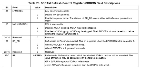
EMIF3A_SDRCR = (0x1 << 31) | // LPMODEN
(0x1 << 30) | // MCLKSTOPEN
(0x0 << 24) | // Reserved
(0x0 << 23) | // SR_PD
(0x0 << 16) | // Reserved
(((unsigned int) ((7.8 * freq) + 0.5)) << 0); // RR
/*SyncReset the Clock to EMIF3A SDRAM*/
PSC1_LPSC_SyncReset(PD0, LPSC_DDR);
/*Enable the Clock to EMIF3A SDRAM*/
PSC1_LPSC_enable(PD0, LPSC_DDR);
EMIF3A_SDRCR &= ~0xC0000000; // disable self-refresh
}
void Set_Core_300MHz()
{
device_PLL0(0,24,1,0,1,11,5);
}
void Set_mDDR_132MHz()
{
device_PLL1(21,1,0,1,2);
DEVICE_mDDRConfig(132);
}
int main()
{
Int16 retval = 0;
// Initialize the board
PSC_All_On_Experimenter();
Set_Core_300MHz();
Set_mDDR_132MHz();
// init the us timer and i2c for all to use.
USTIMER_init();
I2C_init(I2C0, I2C_CLK_400K);
return (int)retval;
}
Again, this code is pretty much taken from verbatim from the GEL file that seems to work properly. Thanks in advance for your help in this matter.
Nick


