This thread has been locked.

If you have a related question, please click the "Ask a related question" button in the top right corner. The newly created question will be automatically linked to this question.

EDMA:L2 to L2 succeeded, but L2 to DDR3 failed

Expert 2985 points
Other Parts Discussed in Thread: TMS320C6670

Hi all,

**********************************************************************************

I want to test the DDR3 bandwidth.

In the beginning, I used the codes below to test if the DDR3 controller's configuration was OK.

    while(1)
    {
        *(DDR3_ADDR) = temp_w;//w
        temp_r = *(DDR3_ADDR);//r
        if(temp_w == temp_r)
            break;
        temp_w++;
        DDR3_ADDR++;
    }

Then the test was OK and I could find the data I wanted to write into the DDR3 using Memory Broswer in CCSv5.3.

**********************************************************************************
Then I tried to use EDMA to move data from DDR3 to DDR3.

My code was based on the EDMA examples in MCSDK and used the SYS/BIOS.

static Int32 EDMA_test (Int32 instNum, Uint8 channelNum);

In the main function, I called this sub function with this code below

EDMA_test(1,6);

means that I used the channel 6 in EDMACC1.

The example code works on ping-pong mode. But I don't need this. So I changed the code to just move data from src to dst.

1.Firstly, I changed the src and dst addresses.   

Uint16 * srcBuff1 = (Uint16 *)0x10800000;//src,L2

Uint16 * dstBuff1= (Uint16 *)0x80000000;//dst,DDR3

2. Secondly, I initialized the data in the src and dst addresses.

    for (loopIndex = 0; loopIndex < 256; loopIndex++)
    {
        srcBuff1[loopIndex] = 0xABCD;
        dstBuff1[loopIndex] = 0;
    }

3. Then the code initialized the EDMA3 module, EDMA3 channel, param set and so on. This part was same as the example codes without any changes.

CSL_edma3Init(&context)

hModule = CSL_edma3Open(&edmaObj, instNum, NULL, &status);

chAttr.regionNum = CSL_EDMA3_REGION_GLOBAL; 

chAttr.chaNum    = channelNum;

chChannel = CSL_edma3ChannelOpen(&chObj, instNum, &chAttr, &status);

CSL_edma3HwChannelSetupQue(hChannel,CSL_EDMA3_QUE_3);

CSL_edma3MapDMAChannelToParamBlock (hModule, channelNum, 2);

 hParamPing = CSL_edma3GetParamHandle(hChannel, 2, &status);

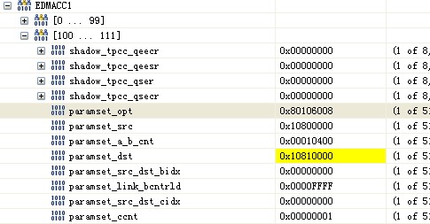
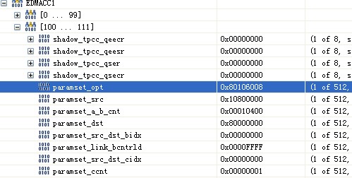
4. After that, I modified the param set. Acnt=256, bcnt=ccnt=1 without LINK.

myParamSetup.option = CSL_EDMA3_OPT_MAKE(CSL_EDMA3_ITCCH_DIS, \
                                             CSL_EDMA3_TCCH_DIS, \
                                             CSL_EDMA3_ITCINT_DIS, \
                                             CSL_EDMA3_TCINT_EN, \
                                             0x6, CSL_EDMA3_TCC_NORMAL,\
                                             CSL_EDMA3_FIFOWIDTH_NONE, \
                                             CSL_EDMA3_STATIC_EN, \
                                             CSL_EDMA3_SYNC_A, \
                                             CSL_EDMA3_ADDRMODE_INCR, \
                                             CSL_EDMA3_ADDRMODE_INCR );
    myParamSetup.srcAddr    = (Uint32)srcBuff1;
    myParamSetup.aCntbCnt   = CSL_EDMA3_CNT_MAKE(256,1);
    myParamSetup.dstAddr    = (Uint32)dstBuff1;
    myParamSetup.srcDstBidx = CSL_EDMA3_BIDX_MAKE(0,0);
    myParamSetup.linkBcntrld= 0xFFFF;
    myParamSetup.srcDstCidx = CSL_EDMA3_CIDX_MAKE(0,0);
    myParamSetup.cCnt = 1;
    if (CSL_edma3ParamSetup(hParamPing,&myParamSetup) != CSL_SOK)
    {
        printf ("Error: EDMA Parameter Entry Setup failed\n");
        return -1;
    }

5. Then I enabled the transfer completion interrupt.

    /* Interrupt enable (Bits 0-1)  for the global region interrupts */
    regionIntr.region = CSL_EDMA3_REGION_GLOBAL;
    regionIntr.intr   = 0x40;
    regionIntr.intrh  = 0x0000;
    CSL_edma3HwControl(hModule,CSL_EDMA3_CMD_INTR_ENABLE,&regionIntr);

6.Triggered the EDMA manually.

CSL_edma3HwChannelControl(hChannel,CSL_EDMA3_CMD_CHANNEL_SET,NULL);

7. Finally, polled the completion interrupt bit.

    regionIntr.region = CSL_EDMA3_REGION_GLOBAL;
    regionIntr.intr   = 0;
    regionIntr.intrh  = 0;
    do {
        CSL_edma3GetHwStatus(hModule,CSL_EDMA3_QUERY_INTRPEND,&regionIntr);
    } while (!(regionIntr.intr & 0x40));


*******************************************************************

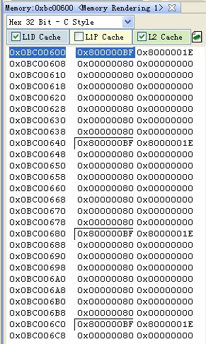
With this codes above I set the src and dst address in L2, the completion interrupt bit raises and I can find the data in the dst.

But the problem is,

When I set the src address in L2 and the dst address in DDR3, the completion interrupt bit raises but I can not find the data in the dst!!

*******************************************************************

So, can anyone one help me? I'll appreciate that!

  • Hi Feng,

    Can you paste the contents of the PaRAM you programmed for the DDR3 transfer? Please take a snapshot just before you manually trigger the EDMA.

  • Hi,

    Thanks for your reply!

    1. Firstly, I set all the src and dst address in L2.

    Uint16 * srcBuff1 = (Uint16 *)0x10800000;//src in L2
    Uint16 * dstBuff1 = (Uint16 *)0x10810000;//dst in L2

    Then I make a breakpoint in the manual trigger code. And I get the param set like the pic below

    After triggering, the param does not change.

    In dst, I can get the data from src.

    2. Secondly, I set the src in L2 and dst in DDR3 like

    Uint16 * srcBuff1 = (Uint16 *)0x10800000;//src in L2
    Uint16 * dstBuff1 = (Uint16 *)0x80000000;//dst in DDR3
       

    Then I also make a breakpoint in the manual trigger code. And I get the param set like the pic below

    After triggering, the param does not also change.

    In dst, I can not get the data from src!!


    *********************************************************************************************

    I don't think my configuration of param set is wrong. Because the EDMA from L2 to L2 is OK. Just the EDMA from L2 to DDR3 or DDR3 to L2 or DDR3 to DDR3 fails.

    Maybe there is mechanism that protect the DDR3 from the operation of EDMA?

    *********************************************************************************************

    Thank you again! Hope you help me!

  • Feng,

    After your L2->L2 transfer, do you clear the event in the Event Clear Register (ECR) before re-triggering the channel for L2->DDR3?

    Did you program the SES MPAX in any way that could have either remapped the default address or changed the protection settings?

    I would check if the secondary event register (SER) or any of the error status registers indicate a problem with the TR.

  • Hi Aditya,

    Thank you first for your reply!

    1. I test the L2->L2 tranfer and L2->DDR3 transfer independently.

    2. I saw the SES MPAX regs just before triggerring L2->DDR3 EDMA like pics below

    I think these values are just the reset values.


    ************************************************************

    No I doubt that there are some problems in the configuration of DDR3 controller.

    In my board, the keystone DSP connects with four DDR3 memory chips. There are four MT41J128M16(16M*16*8 Banks) in my board.

    RAM 0~1: connect with the low 32bits of data line and the CLK1p/n and CKE1

    RAM 2~3: connect with the high 32bits of data line and the CLK0p/n and CKE0

    That means I use the CKE0 and CKE1 in the same time.

    In the GEL file, I set

    NM=0, ROWSIZE= and EBANK=1(means using the CKE0 and CKE1 in the same time)

    But the leveling fails!!

    In this situation, I test the DDR3 using the code like

    *(DDR3_BASE_ADDR++)=0xABCD;

    And I can get the results in the Memory Broswer.

    But if I use the EDMA to transfer data from DDR3 to MSMC, some data will be fault.

    if I use the EDMA to tranfer data from DDR3 to DDR3, I can not get data in the dst.

    So maybe the leveling problems make the EDMA can not write or read the DDR3???

    So is my first setp to solve this problem to solve the leveling problem???


    Feng

  • Feng,

    You had indicated earlier that DDR3 was working as expected, so I assumed the issue would be with s/w programming. Yes, we need to resolve the leveling problem first.

    What is your part number?

  • HI Aditya,

    Thanks!

    So is my understanding right, that when leveling fails this code(*(DDR3_BASE_ADDR++)=0xABCD) can work well just because it writes DDR3 in a very slow frequency, even if the EDMA operation will fail because it will write DDR3 with very tiny delay between two time writing operations?

    Sorry, I can't understand what the "part number" means exactly because of my limited english skills.

    Do you mean which my DSP chip is? or DDR3 chips?

    My DSP chip is TMS320C6670 and there are for MT41J128M16-125E in my board.

    Thanks again!!

    Feng

  • Hi Feng,

    I meant the DSP part number, thanks for confirming. It is possible that isolated reads and writes may work even if leveling failed but it is best to assume nothing will work with full data integrity if it fails.

    (1) When you say leveling failed, does it show a timeout on all three levelings?

    (2) Are you following the initialization procedure recommended in the Keystone DDR3 initialization application note and plugged in the appropriate values in the PHY and register calculation spreadsheets?

    (3) Have you verified that your layout complies with the guidelines in the DDR3 design requirements guide?

    (4) How many boards do you have and how many show this behavior?

    Note: If you have one, you can also verify if your program works as expected on the TI EVM.

  • Aditya said:

    Hi Feng,

    I meant the DSP part number, thanks for confirming. It is possible that isolated reads and writes may work even if leveling failed but it is best to assume nothing will work with full data integrity if it fails.

    (1) When you say leveling failed, does it show a timeout on all three levelings?

    (2) Are you following the initialization procedure recommended in the Keystone DDR3 initialization application note and plugged in the appropriate values in the PHY and register calculation spreadsheets?

    (3) Have you verified that your layout complies with the guidelines in the DDR3 design requirements guide?

    (4) How many boards do you have and how many show this behavior?

    Note: If you have one, you can also verify if your program works as expected on the TI EVM.

    Hi Aditya,

    Many thanks for your such detailed reply!

    (1) After the GEL file is loaded, I see the DDR_STATUS reg and it's value is 0x40000074. This means all the three timeout bits are set.

    (2) I had followed the directions in the PHY and Register excel files to set the initial values of the DDR controller. For example plugged the routing length of the DQS and CLK signals of evey byte lane in the excel files and then get the reg values that should be filled in the SDTIM regs.

    But the leveling also fails.

    But maybe there are some places that I can't  understand very clearly about these regs and values.

    Now I try to check if I followed these directions of the two excel files correctlly. And I must test for several times.

    Then I will give you the feedbacks.

    (3) The board is not design by me. I just see that: every DSP connects with 4 MT41J128M16(16M*16*8 Banks). And

    RAM 0~1: connect with the low 32bits of data line and the CLK1p/n and CKE1

    RAM 2~3: connect with the high 32bits of data line and the CLK0p/n and CKE0

    This is  not the same with the EVM that only using the CLK0p/n and CKE0 to flyby all the 4 DDR3 RAM chips.
     So I set the EBANK bit in DDR_SDCFG reg to use two channels.

    And I will check if it complies with the DDR3 design requirement guidelines as you mentioned.

    (4) We have 2 boards and there are two DSPs in every board. I had tested the two DSPs in one board. The results were the same and the leveling failed. I will test another board.

    Thank you again!

    Feng

  • Hi Feng,

    Feng Jin said:

    RAM 0~1: connect with the low 32bits of data line and the CLK1p/n and CKE1

    RAM 2~3: connect with the high 32bits of data line and the CLK0p/n and CKE0

    This is  not the same with the EVM that only using the CLK0p/n and CKE0 to flyby all the 4 DDR3 RAM chips.
     So I set the EBANK bit in DDR_SDCFG reg to use two channels

    This would have to be corrected. Please have a look at Table 64 in Section 8.1.1.11 "Four 16 Meg x 16 x 8 banks (8.192G bit total)" of the DDR3 design requirement guide. Only CKE0 and CLK0 are to be used for single rank designs. CKE1 and CLK1 are to be used only for dual rank designs and should be left unconnected otherwise.

  • Aditya said:
    This would have to be corrected. Please have a look at Table 64 in Section 8.1.1.11 "Four 16 Meg x 16 x 8 banks (8.192G bit total)" of the DDR3 design requirement guide. Only CKE0 and CLK0 are to be used for single rank designs. CKE1 and CLK1 are to be used only for dual rank designs and should be left unconnected otherwise.

    Hi Aditya,


    1. Do you think this is a really big problem? In our board, the codes like

    while(1)
    {
       *(DDR3_BASE_ADDR++)=0x1234;
    }

    can work well. Only using EDMA to transfer data from DDR3 to DDR3(or L2  to DDR3 or MSMC to DDR3) fails and leveling fails.

    So I don't think there is a big problem in the organization between DDR3 controller and DDR3 RAM chips.

    2. As you mentioned above, I checked the layout and routing details in our board.

    And I found a big problem

    As far as I know, the green line is the correct routing way of  DDR_CLKOUTp/n.

    But in our board, someone(not me) routed the DDR_CLKOUTp/n traces like the pink one! In somewhere of the DDR_CLKOUTp/n, the DDR_CLKOUTp/n branchs two way to the RAMs. Not like the fly-by requirements!

    So my problems that leveling fails and using EDMA to transfer data from DDR3 to DDR3(or L2 or MSMC) fails are relative to this routing error??

    Thank you!

    Feng

  • Hi Feng,

    The pink looks like a balanced-T topology which is used for DDR2. The higher speeds associated with DDR3 require the use of fly-by topology as you have rightly pointed out by the green line. Using balanced-T can cause serious signal integrity problems at DDR3 speeds.

    It is difficult to comment on specific failures that you observe, but TI cannot guarantee a functional DDR3 interface if the design requirements are not followed. The board designer will need to correct this.

  • Aditya said:

    Hi Feng,

    The pink looks like a balanced-T topology which is used for DDR2. The higher speeds associated with DDR3 require the use of fly-by topology as you have rightly pointed out by the green line. Using balanced-T can cause serious signal integrity problems at DDR3 speeds.

    It is difficult to comment on specific failures that you observe, but TI cannot guarantee a functional DDR3 interface if the design requirements are not followed. The board designer will need to correct this.

    HI Aditya,

    Thank you very much  for your patient and very professional replies for helping me to locate the reason causing the problems I met.

    At present, I must lower the DDR3 clock to 400MHz and calculate the CLK line length from controller to each ram chip again. Then I try again to test leveling and EDMA codes. If it fails again, I'll give up to debug further.

    Thank you again!!

    Feng