This thread has been locked.

If you have a related question, please click the "Ask a related question" button in the top right corner. The newly created question will be automatically linked to this question.

New AM1802 Custom Board Bring-up

Other Parts Discussed in Thread: AM1802, TPS650061, AM1808, OMAP-L138, OMAPL138

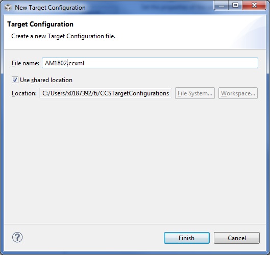
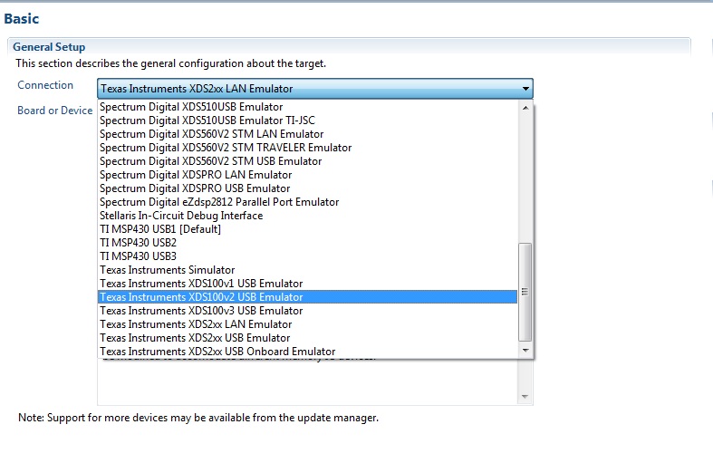
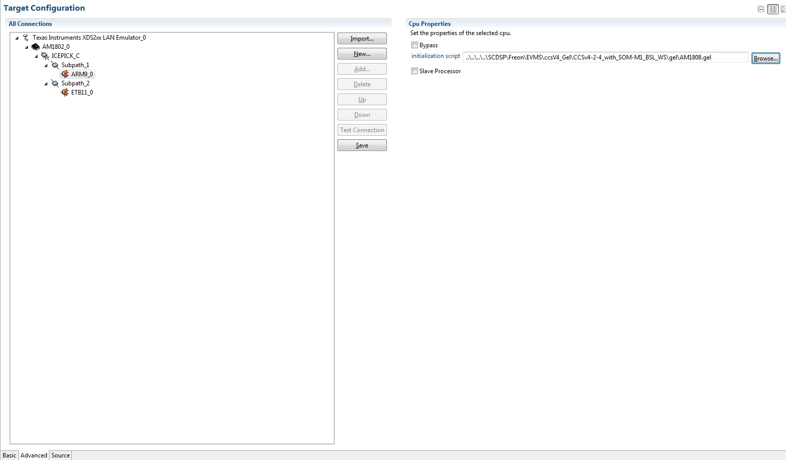
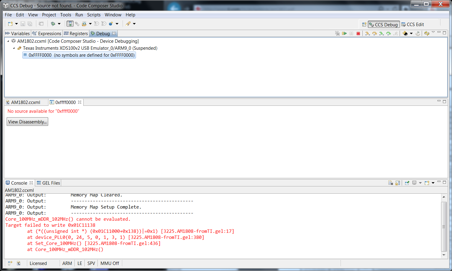
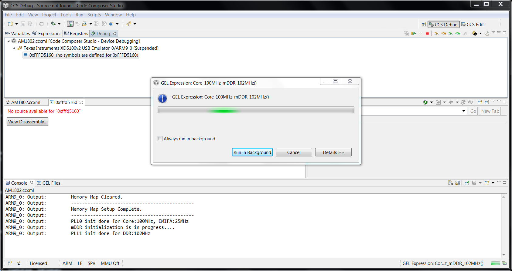
I've got a new board built for the first time and am trying to debug why it isn't showing any real signs of life.

  • I've confirmed the power rails are correct and come up in the correct order
  • I've verified that I have a 25mHz clock at 1.2V
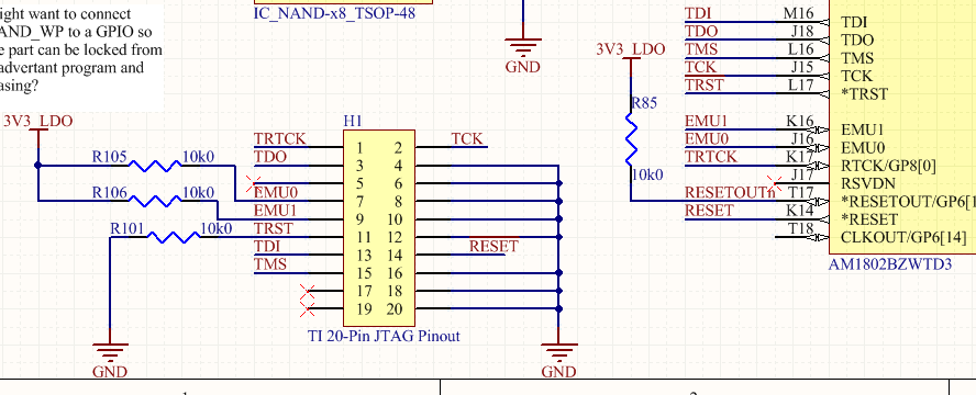
  • I've tied both RESET and TRST to an external switch and held them low then high
  • Boot pins are configured for SD boot (boot[7:0] are 00011100)
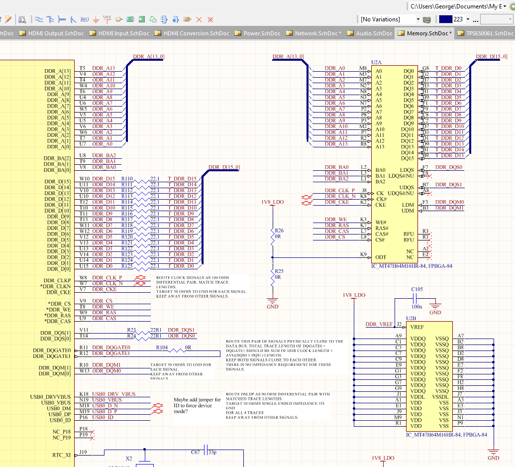
  • uSD socket is connected to MMCSD0 (CLK (ball E9) through 22 Ohm to pin 5)


  • When I power up the board with REST/TRST low I measure a low on the SD clock line. When I pull RESET/TRST high I can see the SD Clock line go high but it isn't generating a clock.
  • I don't see any activity on the CMD line of the SD Card either
  • I have UART1 and UART2 Tx/Rx going to a header but I don't see any activity on those lines either.

Since I see the SD Card clock line go high I know that the processor is doing something but I'm not sure why I don't see a clock signal. I would have also though I'd see something on UART1 (or UART2) Tx line as the ROM loads but I'm not sure about that.

What else can I or should I be checking to see if I can bring this board to life?

Thanks,

George

  • Something that isn't right is that I don't see RESETOUT (pin T17) go low when RESET (pin K14) is pulled low. RESETOUT is pulled high to 3.3V through a 10k resistor.

  • Hi George,

    You have tied both RESET and TRST to an external switch and held them low then high, but basically as per the documentation TRST only needs to be released when it is necessary to use a JTAG controller to debug the device or exercise the device's boundary scan functionality.

    TRST and RESET need to be asserted upon power up, only RESET needs to be released for the device to boot properly. TRST may be asserted indefinitely for normal operation, keeping the JTAG port interface and device's emulation logic in the reset state

    Normally we pull-down the TRST pin on board with 4.7k resistor

    Regards

    Antony

  • Hi Antony:

    TRST is pulled low on the board through a 10k resistor. I will leave it low for my experiments.

    RESETOUT is pulled high to 3.3V through a 10k resistor and is only connected to the Reset input (pin 23) of the Ethernet PHY (DP83848HSQ/NOPB).

    I have not seen RESETOUT ever go low which seems to be telling me that something is wrong. Toggling RESET from low to high I see an increase of current from ~135mA to ~170mA with a 5V input to the board so something is happening. The only sign of life I can see now is the MMC/SD clock line go from low to high and that is not pulled high so the AM1802 is setting it high.

    With a brand new part mounted what else can be checked to see if the part has booted?

    Thanks,

    George

  • Hi George,

    Can you please try connecting the board to CCS through JTAG and run the debug- GEL file to see the desired boot mode settings are latched properly.

    You can refer the below link for downloading the debug gel file

    http://processors.wiki.ti.com/index.php/OMAP-L138_Bootloader

    Regards

    Antony

  • What version of CCS should I install on a Win7 computer?

  • Downloading now, all 1.1GB of it! BTW, the link has a problem because the download file doesn't add the ".exe" extension to the file so you need to rename the file after download before you can run it.

    I've got a Blackhawk USB100v2 JTAG board but I think I need to make an adapter cable. Her's how the connections are but I don't have an actual header mounted on the board (I forgot to order one and the footprint is 1.27mm x 1.27mm dual row and I don't have any of those lying around.

    The board design doesn't control RESET so will JTAG take care of that for me or will I still need to add an external switch to pull it low until after the board is powered up? 

  • OK, CCS 5 is installed and I downloaded the example files you pointed to but I'm having trouble finding a page that tells me how to connect to the board via JTAG and what to do. Would you mind providing some steps or pointing me to the right page please.

  • Hi George,

    If you don’t have the JTAG connector mounted on your board all you need to do is wire wrap between the JTAG connector and to your board

    The board design doesn't control RESET so will JTAG take care of that for me or will I still need to add an external switch to pull it low until after the board is powered up? 

    Does your board have processor supervisory circuit that initiates RESET when you do Power ON?

    Please refer the JTAG pin definition

    http://processors.wiki.ti.com/index.php/XDS_Target_Connection_Guide#Target_Connection_Design

    Please refer the below wiki links to connect AM1802 target to CCS

    http://processors.wiki.ti.com/index.php/How_to_connect_to_the_OMAP-L138/C6748/AM1808_EVM_board_using_CCS%3F

    Regards

    Antony

  • Hi Antony:

    No, unfortunately I forgot to tie RESET into the power up circuit so it is floating on the board. It is brought out to the JTAG header so currently that is where I have attached a pull down and switch. Attached is the schematic review that TI did before we did board layout and they also missed the floating RESET pin.

    Power is ramped up via a circuit using TPS650061 and based on your app note SLVA483 but I forgot to tie the AM1802 reset pin to the TPS650061 reset pin.

    Thanks for the link. I don't see instructions for CC5 nor for the Blackhawk USB100v2 which is odd since that's the one that come's in the experimenter kit. Which JTAG Controller should I select? Are the CC4 instructions the same for the CC5 I have installed?

    For some reason I can't download the AM1808 SOM-M1 GEL, CCS Setup, & BSL Files even thought I'm registered, is there another location I can download files that will work with my board?

    131002-0188-SN_Socius_Schematic review 20131014.xlsx
  • George,

    The wiki link I have shred for CCS Target connection is same for CCS4 vs. CCS5

    You can select Texas instruments XDS100v2 emulator the USB100v2 is a TI XDS100v2-compatible emulator fully supported under CCS v4 and future Texas Instruments roadmap software development environments.  

    Attached the screen shot for your reference

    Logic PD website is the only source for AM1808 SOM- M1 GEL, CCS Setup, & BSL Files you can request logic PD technical support for assistance .

    But the reset pin should be kept low during power up once the voltages and clocks are stabilized you need to release it.

    First try connect the target and run the debug gel file, once you succeed running the debug gel file on target you can see the status of the boot pins,PLL settings …etc  

    Then you can give a try from some sample programs form Logic PD examples

    Regards

    Antony

  • OK, thanks for confirming that CC4 and CC5 can use the same instructions. I've sent an email to Logic PD support so hopefully they get back to me quickly. Not sure why I can't d/l because I've downloaded all their design files when I first started.

    I'll keep the external switch to control reset and hopefully I'll be able to see something with the debug gel file.

    One other thing I've noticed is that my boot configuration resistors are weak (100k) and I read that they should be stronger but maybe that has changed in the newer silicon. I've measured the voltages and they are as expected for SD boot. If I should change them I'd like to use values already on the board in order to keep cost down. I've got the following choices:

    1.0k

    1.5k

    2.2k

    10k

    47k

    I guess if JTAG is able to connect to the board I'll be able to read the registers and see if they are as expected. If they are then 100k should be OK, right?

  • Hi George,

    Nomally we use 4.7k Pull-Up/Down resistor for boot pins ,but at the same time we are not recommending weak pull-up/down.

    You can use 2.2K just in case if the boot pins are not latched properly.

    Yes, once you connect the target using Gel script you shoul be able to read the registers

    Regards

    Antony

  • Hi Antony:

    I'm sorry but have you actually tried to follow these instructions when you have CC5? I go to

    http://processors.wiki.ti.com/index.php/How_to_connect_to_the_OMAP-L138/C6748/AM1808_EVM_board_using_CCS%3F#XDS100v2.2C_XDS510_or_XDS560_external_emulator_-_ARM_only_.28AM1808_SOM.29

    and the first thing it says is to not follow these instructions but

    For XDS100v2 you can use the configuration that comes ready in the BSL instead of following the steps below. The configuration file is at ...\1016316A_AM1808_BSL\AM1808_BSL\src\bsl\AM1808.ccxml. Also, you can see sections 6 and 7 of the Zoom™ AM1808 Development Kit User Manual

    So I open that document, scroll to page 12 but the directory structure doesn't match what they show (ignoring the root). I manage to load the BSL file (which is the AM1808.ccxml file, or at least I hope it is). Now the LogiPD instructions go on to say to load some test files but I don't want to run tests I just want to connect and read some registers. I look back at the original page and none of those screen shots look familiar when you're running CC5. As an example, in their pictures you have Basic, Advanced, and Source in the bottom left corner but I don't have that.

    Not only that but in CC5 I haven't done anything but load that gel file and it already says that I have 2 errors:

    Cannot find a driver for Cpu PRU_0

    Cannot find a driver for Cpu PRU_1

    Could you please help sift through all of this and let me know how I can use CC5 and probe my board. At this point I don't know what document or page to follow because nothing seems to match the instructions.

  • I made a little progress by double clicking on the ccxml file and that showed me the page with the Advanced settings.

    I don't think ICEPICK is supposed to be there is it?

  • George,

    ICEPICK should be there under the sub patch select ARM9 and  load the debug gel file in the initialization  script  path and save it.

    Before connecting the target you can check the JTAG connection by pressing the Test connection options.

    Once you succeed then connect the target by right clicking on the .ccxml  file and  select the launch selected configuration

    Regards

    Antony

  • Hi Antony:

    OK, well I thought ICEPICK was a different hardware than my JTAG controller. When you say load the debug gel file, which file are you referring to? The download from LogicPD has 3,414 files in 1,036 folders. By process of elimination I'm thinking it's in one of these directories:

    ARM BSL

    OMAP-L138_GEL_BSL_Files

    gel

    But which one and which file? Does it matter that their eval kit is for the AM1808 and my board has a AM1802?

    I'm not sure I have the right file loaded but I have run the Test connection and it fails. The light on the JTAG board is ON and there is a XDSSerial command that reports that it sees the controller.

    I have run the tests with the controller connected to my board so I can try again without it connected. The errors are referencing something about FTDI drivers but Device Manager doesn't show any problems.

    George

  • I disconnected the JTAG Controller and ran TEST Connection and the software reports that I need to be connected to the target.

    See attached error information and a screen grab showing those error messages I mentioned last night

  • When I power up the board, select ARM9_0, and then click on the test connection button I get an error

    -----[An error has occurred and this utility has aborted]--------------------

    This error is generated by TI's USCIF driver or utilities.

    The value is '-154' (0xffffff66).
    The title is 'SC_ERR_FTDI_WRITE'.

    The explanation is:
    One of the FTDI driver functions used to
    write data returned bad status or an error.

    See attached file for full details of the test.

  • We took a closer look at the AM1802 using the 3D X-Ray and found some opens. We built a new board last night and with a confirmed good soldering job I now see some traffic on the SD clock line as well as some traffic on the SD data line.

    I need to make a new JTAG adapter cable since I had to unsolder my wiring mess so the new board is configured to boot from SD.

    I don't see any traffic on either UART1 or UART2 Tx/Rx which puzzles me. Do you have any ideas on what could prevent seeing anything. I would think that even if the processor is not configured properly I would still get some initial messages out the serial port.

    I've wired up the reset line to the TPS650061 rest pin (pin 20). The rest signal looks good and releases about 25ms after the 3.3V rail comes up. My only concern is that pin 20 of the TPS650061 is being pulled high to the 1.8V output so the AM1802 is only going to see a 1.8V signal. This seems to be working as I see the resetout signal of the AM1802 (T17) release but I wanted to know your thoughts on this and if the production board should be changed to a 3.3V level?

  • We finally made it past the JTAG issues and have successfully run the debug GEL tests. We also were able to run the UART test but have failed both the SD Card and RAM test. I'm not sure but I think the SD Card test might be using RAM for the FIFO so failing the SD Card test could be related to the RAM test failure.

    I have gone through the spreadsheet timings and came up with values of:

    DRPYC1R  0x000000C6

    SDCR:  0x00134A32

    SDTIMR1:  0x26522A09

    SDTIMR2:  0x3C14C722

    SDRCR:  0x00000492

    I edited the AM1808 initilization program with these changes and watched the registers as I stepped through the code. I can see the code step into my changes but I don't see the actual register values change. I'm not sure why this is happening.

    The AM1808 SOM uses Mobile SDRAM (Micron MT46H64M16LFCK-6:A) according to the BOM but we are using DDR2, Micron MT47H64M16HR-25:H so I would expect the RAM test to fail if the registers are not configured properly.

    Attached is my worksheet for reference6175.GI-mDDR_DDR2_Memory_Controller_Register_Calc_Rev4.xlsx

    Is there another way to do a simple DDR test and/or SD test?

  • Hi George,

     Can you please send us the debug gel CCS console output?

    And also try connecting the target using the Gel script attached, once you connect the target go to script option in CCS Menu- Script- Frequency settings-and select CORE200Mhz_ …once you did it the next step is go to view option and select memory browser and type 0xc0000000 and press go once you see the memory view try typing some values in the browser window and see the value’s get updated.

    3225.AM1808.gel

    Regards

    Antony

  • Hi Antony:

    Attached is the debug gel output. I'll try your gel file now.... This is the error I get with your gel file and it's the same error I was getting earlier.

    Core_200MHz_mDDR_126MHz() cannot be evaluated.

    Could not read 0x01C1417C: Target is not connected

    at (*((unsigned int *) (0x01C14000+0x17C))&=~(0x00000010)) [3225.AM1808-fromTI.gel:223]

    at device_PLL0(0, 24, 2, 0, 1, 7, 3) [3225.AM1808-fromTI.gel:376]

    at Set_Core_200MHz() [3225.AM1808-fromTI.gel:430]

    at Core_200MHz_mDDR_126MHz()

    George

  • I played around this afternoon with it and for a few times I was actually able to bring up the memory view and change some values. I was confused why when I changed one location it seemed to change 2 locations. I closed the session and power cycled but now I just keep getting the error message that I posted.

    I think this has to do with how my project is set up and the steps I am taking. I've tried so many different things just to get to where I am now that nothing is clear as to what actually needs to be done. Now that I know a little more than I did last week can you provide a project that you would work with an AM1802 board and the steps I need to reliably reproduce this testing environment. I want to be able to confirm that DDR2, NAND, and the SD card are working. Our design follows the LogicPD with the exception of using the AM1802 processor and using DDR2 instead of mDDR. I would think that I could just change the gel script and use their test programs but as you know I'm not having much luck. I was hoping to just create a boot SD card and go from that but I'm not that lucky.

  • Hi George,

    According to the debug gel console output everything looks fine for me.

    However few times you’re able to bring up the memory view and afterwards it shows error message.

    Have you tried Core_100Mhz_mddr2_102MHz….?

    I don’t see there is much difference between DDR and LPDDR it should work with the same Gel script.

    Can you please try re-calculating the DDR timing values with the spreadsheet from the below wiki link

    http://processors.wiki.ti.com/index.php/File:SYS_CLK_CALC_OMAP-L138_C674X_AM18X_v1p0.zip

    Please check the DDR connection once (Schematics & Layout), power and clocking.

    Once the DDR is up we will able to test other interfaces quickly.

    Check Debugging guide

    http://processors.wiki.ti.com/index.php/OMAP-L138_Hardware_Design_Guide

    Regards

    Antony

  • Hi Antony:

    Is your spreadsheet different than the one I attached a few posts ago?

    I don't think Ihave a hardware issue but I'm thinking that CCS is messed up. I've tried so many different things to get it working I'm not confident that it is configured correctly and I cannot find any clear instructions on what I can do to wipe everything out and start with a clean environment and try the latest tests again.

    I've gotten it to write to the memory once (or so I believe) so that should tell me that the board is designed properly. I've reviewed the design as well as TI so I'm really thinking this is all CCS issues.

    Can't you provide some simple steps to ensure that CCS is correctly configured for a board with a AM1802?

    George

  • Hi George,

    Here is the steps

    1. Open the CCS and go to File-New- Target configuration File (Step1)
    2. Once the new target configuration window opens give the target name AM1802 and click finish button (Step2)
    3. In the basic option window select the right emulator you are using from  the drag down menu (Step3)
    4. Then select the device AM1802 once you done press the save button  (Step4)
    5. Then press advanced tab in the same below and select the ARM9 core and point the AM1808 initialization script in the right side of the window ,once you done press save button (Step5)
    6. You can go to view-target configuration file to view your target configuration visible it will display as AM1802.ccxml  (Step6)
    7. Right click the target configuration and select  set as default option ,then right click again and select launch target configuration  (Step7)
    8. Once you see the ARM9 target  in the Debug menu as disconnected, Right click on the target ARM9_0 and select connect target
    9. Then go to script menu and select the frequency options Core_100MHz…

    Regards

    Antony

  • OK perfect, this is what I wanted so I'll follow this. One question I forgot to ask. At this last step when I right click and connect to target I was always seeing it connect and then it would show as suspended and I wondered if that was a problem or just the state it puts it in after it connects. Can you show me a screen shot of what it looks like after you connect?

    Thanks,

    George

  • Hi George,

    It is just the state it puts it in after it connects

    Regards

    Antony

  • Once I connect I see a window open up that says "No source available for "0xfffd5160"

    I ignore that error and proceed to set the frequency and I get the error I've been except for that 1 time it appeared to work

  • What doesn't make sense to me is that I'm able to read from the CPU using the debug gel scripts 100% of the time. I'm also able to run any of the other scripts as shown below. From my understanding the other scripts are writing to the CPU registers just like the set frequency is supposed to do yet the set frequency returns an error as though it's not able to access the DDR registers at 0x01C11138 and that seems to tell me that something is not configured correctly or my understanding of what the scripts are doing is incorrect.

    Is the memory map different between the AM1802 and the AM1808??

  • OK, I may have found the problem or I'm just lucky this time connecting to the target. I changed my JTAG to use adaptive frequency and this time it connected.

    If I enter 0xc0000000 in the Memory Browser and hit GO I do see values in memory. I moved to 0xc0000004 and changed it to 55555555 and hit enter but locations 0xc0000000 and 0xc0000008 are then changed to 55555555 and 0xc0000004 reverts back to the original value I believe.

  • Hi George,

    Can you redue the JTAG clock frequency and check once.

    Regards

    Antony


  • So this behavior is not normal? I'll reduce the frequency down to maybe 100kHz and try again. 

    I didn't go as low as 100kHz but I'm getting the same result I don't see anything wrong with the connection between the DDR2 and the AM1802:

  • I was reviewing the GEL file you provided and I believe that the RAM configuration is not compatible with the DDR2 I have on my board. As a quick test I was able to connect and using the memory browser I modified the SRAM successfully (0x80000000).

    I made the following changes to your GEL file but I get errors when it loads. I'm a little confused why there are 3 different memory enable registers (MSDRAMEN, DDR2EN, SDRAMEN). I would expect that to just be a single bit register with something like 0 for mDDR and 1 for DDR2 so since I don't understand the relationship between these register bits perhaps that where my error is. The TRM isn't much help as it just states that the enables DDR2, DDR, and SDRAM and they are used together?

    Here's my changes:

     EMIF3A_SDCR = (EMIF3A_SDCR & 0xF0000000) |  // Reserved
                      (0x1               << 27)  |  // DDR2TERM1
                      (0x0               << 26)  |  // IBANK_POS
                      (0x0               << 25)  |  // MSDRAMEN GI Changed from EVM
                      (0x0               << 24)  |  // DDRDRIVE1
                      (0x0               << 23)  |  // BOOTUNLOCK
                      (0x0               << 22)  |  // DDR2DDQS
                      (0x0               << 21)  |  // DDR2TERM0
                      (0x1               << 20)  |  // DDR2EN GI Changed from EVM
                      (0x0               << 19)  |  // DDRDLL_DIS
                      (0x0               << 18)  |  // DDRDRIVE0
                      (0x1               << 17)  |  // DDREN
                      (0x1               << 16)  |  // SDRAMEN
                      (0x1               << 15)  |  // TIMUNLOCK
                      (0x1               << 14)  |  // NM
                      (0x0               << 12)  |  // Reserved
                      (0x3               << 9)   |  // CL
                      (0x0               << 7)   |  // Reserved
                      (0x3               << 4)   |  // IBANK GI Changed from EVM
                      (0x0               << 3)   |  // Reserved
                      (0x2               << 0);     // PAGESIZE

  • The recommended method for getting the right EMIF values is to utilize this wiki page:

    http://processors.wiki.ti.com/index.php/Programming_mDDR/DDR2_EMIF_on_OMAP-L1x/C674x

    You should use the spreadsheet on that page in conjunction with the data manual for the specific DDR2 device that you put on your board.  You need to enter the clock speed to which you configured the PLLs as well as all the timing parameters from the DDR2 data manual in order to come up with the appropriate EMIF configuration.  You should make sure the values being programmed by the gel file agree with the values being generated by the spreadsheet.

    George Ioakimedes said:
    I'm a little confused why there are 3 different memory enable registers (MSDRAMEN, DDR2EN, SDRAMEN)

    Details of how to program those fields is given in the TRM in Section 14.2.13 Auto-Initialization Sequence.

  • Yes, I've used that spreadsheet and attached it in an earlier post but earlier in this thread I was told "I don’t see there is much difference between DDR and LPDDR it should work with the same Gel script" so I didn't go through the GEL script and verify everything as I was told that it should work.

    According to my review of the Micron MT47H64M16HR-25:H datasheet and using the spreadsheet I come up with the following register values:

    SDCR 0x00134A32
    SDRCR 0x00000492
    SDTIMR1 0x26522A09
    SDTIMR2 0x3C14C722
    DRPYC1R 0x000000C6

    I'll review my GEL changes that I posted above compared to this and see if I missed something. I know my timings are different than what the GEL script currently uses but I don't think a timing value should cause the memory write changes I'm experiencing.


  • If I try to load my latest GEL file and choose one of the frequency scripts it will start to run but then CCS just hangs. I noticed this hanging issue other times so I went back the GEL file provided and I find that I can run the frequency script once but if I try to run it again or run a different frequency script CCS will hang the same as it does with my script.

    Is there really not a debug GEL script for DDR2 that is known to work? It seems odd to me that there wouldn't be since the part supports it and the part has been available for many years.

  • The original OMAPL138/AM1808 EVM used LPDDR and that's why the gel file configures LPDDR.  Luckily there's another board called the LCDK which uses DDR2 (though not the same exact part so the timings will vary).  The User's Guide is here:

    http://processors.wiki.ti.com/index.php/L138/C6748_Development_Kit_%28LCDK%29

    Further down that page I found the following link to its gel file:

    http://processors.wiki.ti.com/images/6/61/Lcdk_ccs_gel.zip

    There's a note saying this gel file ships in recent versions of CCS so you may already have it...

    Keep in mind these gel files are meant for a specific board.  TI customized the setup for our eval boards, but you need to make corresponding adjustments for your own hardware.  So if you used a different speed input clock then your PLL calculations will look different than ours.  If you used a different DDR2 device then the timings for that device won't match exactly with ours.  It is expected that you will make these adjustments to account for the decisions you made in creating your hardware.

  • George,

    Recently you’re able to bring up the memory browser window and changed some values in the DDR memory location but other location gets changed instead of intended location.

    Now again you’re facing the target connect issue when you do the frequency settings in the gel script, I hope you’ve already resolved this issue by using adaptive frequency in JTAG connection …?

    Please check the similar kind of post for the DDR2 configuration.

    http://e2e.ti.com/support/dsp/omap_applications_processors/f/42/t/116609.aspx

    This customer resolved the issue by changing the RL value in the DDR PHY control register

    The Read Latency (RL) needs to be greater than CL by ateast 1.

    The datasheet suggests a min RL = CL+1 and a max RL =7.

    Configuring RL to 7 has resolved this issue

    Please cross check with your settings, but make sure the timing values are aligned with respect to your memory datasheet

    Regards

    Antony

  • OK, I'm getting closer with changes to the GEL file. I need to try this latest post about RL, and try that.

    I remember seeing that LCDK board and the GEL files and I had downloaded and tried it but I believe that was before I got JTAG working.

    When you look at Registers in CCS where do the names come from? They are slightly different than the GEL file, TRM, and spreadsheet. As an example, SDTIMR1 is SDTIM1 in CCS and searching for DRPYC1R returns nothing.

    I'm fairly confident at this point it's a configuration issue because I can change memory but now it changes in different locations.

    Also, I just noticed that when using the spreadsheet once you enter values on the RegCalc page the calculated register value is not linked to the RegDecode page which I didn't catch before.

  • OK, I would now say that I am finally at a point where I can test the RAM. I loaded the LCDK OMAP-L138 GEL file and with that GEL I am able to write to the correct RAM location. I was also able to load the ARM eXp RAM TEST and that successfully passed.

    I'll review the LCDK GEL file and compare it to my latest attempt but hopefully this will help anyone else who decides to use DDR2.

    I still need to test NAND and SDMMC but those are connected just like the EVM so hopefully now that RAM is configured properly those will also pass.

  • Well my joy didn't last too long. I moved on to trying to test my NAND and I didn't get too far. Looking at the OMAP-L138_C6748 LC Dev Kit Ver A6a.pdf schematic I confirmed that my NAND is connected to the same pins however I am using a x8 vs x16 and my NAND is from Spansion (S34ML04G100TF1000), not Micron (MT29F4G16ABADAH4).

    Looking through the LogicPD NAND test I saw that it checks for MFG_ID so I changed that. I also changed the configuration for a x8. NAND parts are fairly universal as far as timing goes so I would think that the timing settings would be OK.

    I used the pin mux utility program and with those values I added a script to the OMAP-L138_LCD.gel file with the following:

    hotmenu SOCIUS_PINMUX() {
        PSC0_LPSC_enable(0, LPSC_EMIFA);
        PINMUX0        = 0x44111811;
    	PINMUX1        = 0x00011001;
    	PINMUX2        = 0x88888888;
    	PINMUX3        = 0x88888888;
    	PINMUX4        = 0x22222288;
    	PINMUX5        = 0x00111100;
    //	PINMUX6        = 0x10110010;
        PINMUX7        = 0x10110010;
    //	PINMUX8		   = 0x11111111;
        PINMUX9        = 0x11111111;
    	PINMUX10        = 0x80222222;
    //	PINMUX11        = 0x10110010;
        PINMUX12        = 0x01100000;
    	PINMUX13        = 0x88888801;
    	PINMUX14        = 0x00000088;
    //	PINMUX15        = 0x10110010;
    	PINMUX16        = 0x88888800;
    	PINMUX17        = 0x00000088;
    	PINMUX18        = 0x00000000;
    	PINMUX19        = 0x08888800;
    	
        EMIFA_ACFG3   |= 0x0; //Set NAND to 8-bit
        EMIFA_NANDFCR  = (EMIFA_NANDFCR & ~0x30) | 0x12;
     
        GEL_TextOut("\tAll Pins Configured for Socius.\n","Output",1,1,1);
        GEL_TextOut("\t---------------------------------------------\n","Output",1,1,1);
    }

    In the gel file is also a script to setup EMIFA for a NAND connection whichhas the following:

    hotmenu EMIFA_NAND_PINMUX() {
        PSC0_LPSC_enable(0, LPSC_EMIFA);
        PINMUX7        = (PINMUX7 & ~0x00FF0FF0) | 0x00110110;
    	PINMUX8		   = 0x11111111;
        PINMUX9        = 0x11111111;
        PINMUX12       = (PINMUX12 & ~0x0FF00000) | 0x01100000;
        EMIFA_ACFG3   |= 0x1;
        EMIFA_NANDFCR  = (EMIFA_NANDFCR & ~0x30) | 0x12;
     
        GEL_TextOut("\tEMIFA Pins Configured for NAND.\n","Output",1,1,1);
        GEL_TextOut("\t---------------------------------------------\n","Output",1,1,1);
    }

    What I do is run the frequency setting, then EMIFA, then my script. Once those are done I run the ARM EVM NAND Test which was compiled after I changed the MFG_ID in the evmam 1808_nand.c file (located in the ARM BSL\src directory) like this:

    // expected device id for Micron MT29F4F08AAC.
    //#define EXPECTED_MFG_ID                (0x2C)
    //#define EXPECTED_DEV_ID                (0xDC)
    
    // expected device id for Spansion S34ML04G100TF1000.
    #define EXPECTED_MFG_ID                (0x01)
    #define EXPECTED_DEV_ID                (0xDC)

    Can you think of something that I might have missed in order to test the NAND?

    Thanks again for your help!

    George

  • George,

    Others may disagree, but in my opinion I would only use CCS, gel files, and test projects for the purpose of testing out the DDR (like you have done).  Once you get beyond the DDR and into things like the NAND flash I find it's a much better use of time to start using u-boot.  There are a lot more "smarts" built into u-boot so ultimately it requires less work to get things working, and that work is reusable (i.e. your end product will likely use that same code from u-boot).  At least in my experience I see a lot of people spending a lot of time with these various test projects and then they set those projects aside and never touch them again.  Better off to just invest the effort in the "real" software.  If you're looking for some really low-level validation, perhaps just see if you're able to read back the ID or something trivial from the NAND flash, but leave the erasing, flashing, etc. to u-boot which is well-equipped for that sort of thing.

    Also, respectfully, this thread is getting too long.  Please start unique threads for each issue you encounter as you do your board bring-up.  This thread is becoming a hodge podge of topics which makes it less useful to others.  Thanks!  :-)

    Brad

  • Hi Brad:

    Thanks again. Yes, I wasn't expecting to run into so many issues and was hoping for something like the LCDK gel after my 1st post.

    I actually did start with trying to create a boot SD card and was hoping to use that. I have a thread started at http://e2e.ti.com/support/dsp/omap_applications_processors/f/42/p/314721/1097791.aspx#1097791.

    When that card didn't boot I thought maybe I better back up and verify some fundamentals. Using CCS I have confirmed that DDR and UART are working so I'll jump back on that other thread and perhaps you can help determine why I wasn't able to see any boot messages when trying to boot from SD.

    Thanks,

    George