This thread has been locked.

If you have a related question, please click the "Ask a related question" button in the top right corner. The newly created question will be automatically linked to this question.

How to enable data read and write permission for DDR2 ?

Other Parts Discussed in Thread: OMAPL138

Hi,

     How to enable data read and write permission for DDR2 ?

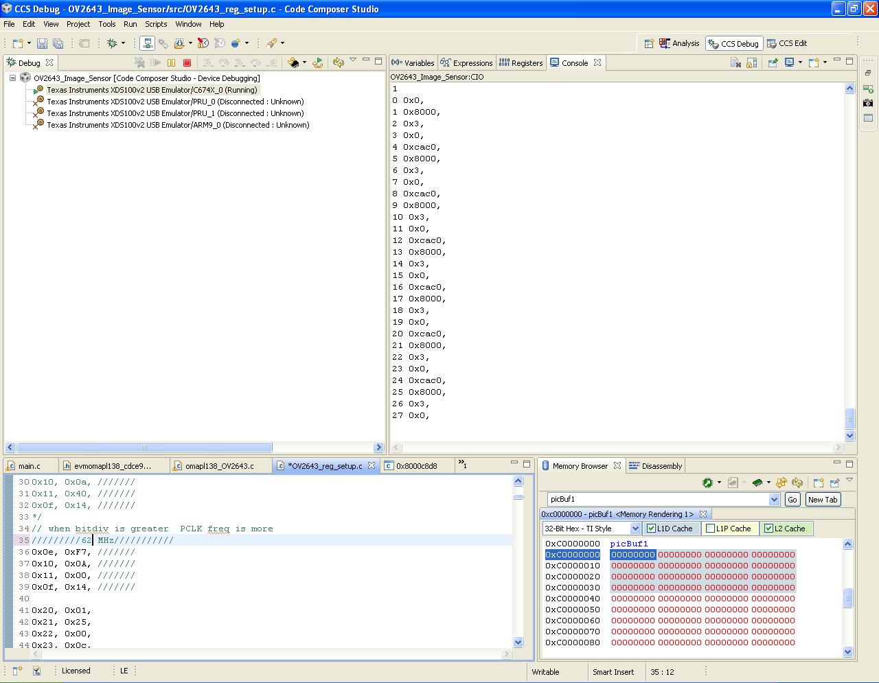
I have set data section to DDR2 ( 0xC0000000 - 0xCFFFFFFF ) to store the data acquired VPIF DMA0 and VPIF DMA1 .

In the Memory Browser tool of CCS doesn't show the data, but prints 4 values repetitively when programmed to print.


  • Hi Vaishak,

    Thanks for your post.

    OMAPL138 has a Memory Protection unit(MPU) that can be configured to manage access to memory from system masters. The MPU can record a detected fault, or invalid access, and notify the system through an interrupt. There are two MPUs on the device (MPU1 and MPU2). MPU1 is used to protect/manage access to shared ram while MPU2 is used to manage access to DDR2/mDDR. Please refer to chapter 6 in Technical reference guide for more information.

    You might also be interested in looking at the sample code (C6748_mpuTest.zip) we have distributed on this forum thread below that demonstrates this functionality using MPU2:

    http://e2e.ti.com/support/dsp/omap_applications_processors/f/42/t/158135.aspx

    Also, there is some MPU test project in the below E2E thread which prevents the DSP from accessing external DDR memory that is being used by the ARM:

    http://e2e.ti.com/support/dsp/omap_applications_processors/f/42/t/291838.aspx

    Thanks & regards,

    Sivaraj K

    ------------------------------------------------------------------------------------------------------- 
    Please click the Verify Answer button on this post if it answers your question.
    --------------------------------------------------------------------------------------------------------