This thread has been locked.

If you have a related question, please click the "Ask a related question" button in the top right corner. The newly created question will be automatically linked to this question.

AM335x USB Overcurrent VBUSDRV

Hi i am trying to implement a custom computer on Module in the SMARC specification in which we have 2 USB host. But in the SMARC Specification USBx_EN_OC# pins are multimode pins (VVBUS Enable and Overcurrent implemented on same pin). 

  • The Module drives USBx_EN_OC# low to disable the power delivery to the USBx device.
  • The Module floats USBx_EN_OC# to enable power delivery. The line is pulled to 3.3V by the Module pull-up, enabling the Carrier board USB power switch.
  • If there is a USB over-current condition, the Carrier board USB power switch drives the USBx_EN_OC# line low. This removes the over-current condition (by disabling the USB switch enable input), and allows Module software to detect the over-current condition.
  • The Module software should look for a falling edge interrupt on USBx_EN_OC#, while the port is enabled, to detect the OC# condition. The OC# condition will not last long, as the USB power switch is disabled when the switch IC detects the OC# condition.
  • If the USB power to the port is disabled (USBx_EN_OC# is driven low by the Module) then the Module software must be aware that the port is disabled, and the low input value on the port does not indicate an over-current condition (because the port power is disabled).

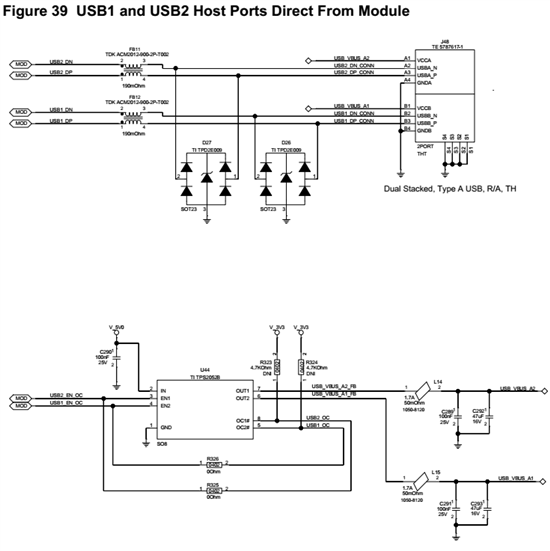
At the carrier side the following implementation is made

How do you suggest i implement the module side design based on the specification given below?

  • The USB subsystem in AM335x expects the VBUS power switch enable inputs to be connected to the respective USBx_DRVVBUS outputs.  These outputs will be driven high when software begins a USB session if the respective USBx_ID terminal is connected to ground with less than 10 ohms which is used to indicate the USB port should operate as host and it does not detect VBUS already present.

    Also note, the USBx_DRVVBUS outputs on AM335x are push-pull so they cannot be directly connected to the VBUS power switch OC# open-drain outputs as shown in the SMARC specification.

    The USB subsystem in AM335x monitors the VBUS voltage level to determine if there is an over-current condition.  If there is an over-current on VBUS, the USB power switch will go into current limit and the voltage will drop.  If the over-current condition causes VBUS to drop below 4.4 volts, the AM335x device will generate an over-current interrupt and software should disable the VBUS power switch.  Therefore, looping the OC# outputs back to the enable inputs is not necessary for detecting an over-current condition.

    Also note, VBUS must be controlled by USBx_DRVVBUS when operating as USB host.  The USB OTG controller used in AM335x can be configured to operate as USB host or USB peripheral.  When operating as USB host, it does not expect VBUS to be applied before it drives USBx_DRVVBUS.  If it detects VBUS present when a host session is started it assumes another host may be connected so it automatically begins operating as USB peripheral.  Therefore, you can not  connect VBUS to a 5 volt source not controlled by USBx_DRVVBUS.

    The AM335x USBx_ID terminal is not a digital input.  Please read Note 9 attached to the Absolute Maximum Ratings table in the data sheet for a more detailed description of these terminals.

    Regards,
    Paul

  • If USB Overcurrent is detected by AM335x by monitoring the VBUS line, then why AM335x_USB1_OC connected to pin B12 in AM335x STK design schematic. Is it used as an interrupt?

    Regards,

    Paul

  • I would like to know 

    Can we use RGMII2 functionality along with USB0 as a host?

  • I discussed this with the board designer and he said the USB power switch OC# output was connected to a GPIO just in case someone wanted to use it.

    The USB0_DRVVBUS signal function is not required on this board since USB0 is configured to only operate as USB peripheral, so he used the GPIO function of this terminal such that it could be configured as an interrupt input.

    Some of the AM335x requirements mentioned in my previous post and the SMARC requirements make it difficult to design a product that meets both requirements.  For example, AM335x needs to monitor VBUS and the SMARC definition does provide a module connection to USB1 VBUS.

    However, I may have a suggestion for combining the USBx_DRVVBUS and OC# signal functions. Connect the combined signal from the carrier card to a 3.3 volt AM335x GPIO with the GPIO configure to operate as an open-drain by permanently setting the output low and toggle the output enable to go between driven low and high-Z mode.  The 3.3 volt pull-up resistor described in the SMARC specification could be connected to the USBx_DRVVBUS output.  This would result in this signal being low if either the GPIO output enable is active or the VBUS power switch OC# output is active even when USBx_DRVVBUS is driven high. However, the signal will never go high until the USBx_DRVVBUS signal connected to the pull-up goes high.  Note: you may need to have a week pull-down connected to this signal so it is not floating when it is not driven by one of the three sources.  You can configure the GPIO to detect a negative edge transition and generate an interupt if you want to use the GPIO as the over-current interrupt rather than the one provided by the USB subsystem.

    For USB1, you may need to implement a circuit on the module that forces VBUS to 5 volts when USBx_DRVVBUS goes high and use the approach described above to monitor the over-current status of the carrier board VBUS signal.

    Regards,
    Paul

  • Thank you Paul for the comprehensive reply.

    Sorry for mouse pointer. DIR is connected to ground and VCCB to 3.3.V rail. Do you think adding this circuit to SMARC configuration given above work?

    Regards

    Paul

  • This should work and it is nice to see you planned to use another TI device.  However, I would also consider using a discrete circuit with two FETs and a pull-up resistor which may provide a lower cost solution.

    You can use a P-channel FET as a power switch by inserting it in series with the 5 volt source and AM335x VBUS terminal.  Then use a N-channel FET to invert the DRVVBUS signal and drive the P-channel gate by connecting the N-channel drain to the P-channel gate along with a pull-up to the 5 volt source.  Then connect DRVVBUS directly to the N-channel gate with the N-channel source connected to ground.

    The AM335x VBUS terminal has a minimum input impedance of 40k ohms so you can use a low current P-channel FET for the power switch.

    Regards,
    Paul

  • I hope this circuit will work as you had suggested.

    Regards,

    Paul

  • Yes, this circuit should work.

    Regards,
    Paul