This thread has been locked.

If you have a related question, please click the "Ask a related question" button in the top right corner. The newly created question will be automatically linked to this question.

AM335x GPMC phantom chip select generation

Other Parts Discussed in Thread: AM3357, SYSBIOS

Hi,

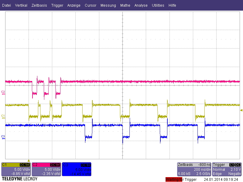
We use the GPMC module in the AM3357 accessing an asynchronous Dual Port RAM (16Bit databus).

We write three values as you can see below:

  //### Test
  *((volatile unsigned short *)(0x09000004))=0x0001;
  *((volatile unsigned short *)(0x09000006))=0x0002;
  *((volatile unsigned short *)(0x09000008))=0x0003;
  //asm(" DMB");
  //### Test Ende

The writes itself work as it should. If we watch the signals on an oscilloscope we see that the chip select signals goes low for 8 times and only for the expected 3 times the WEn signal goes low. We would expect the chip select signal to go low only 3 times.
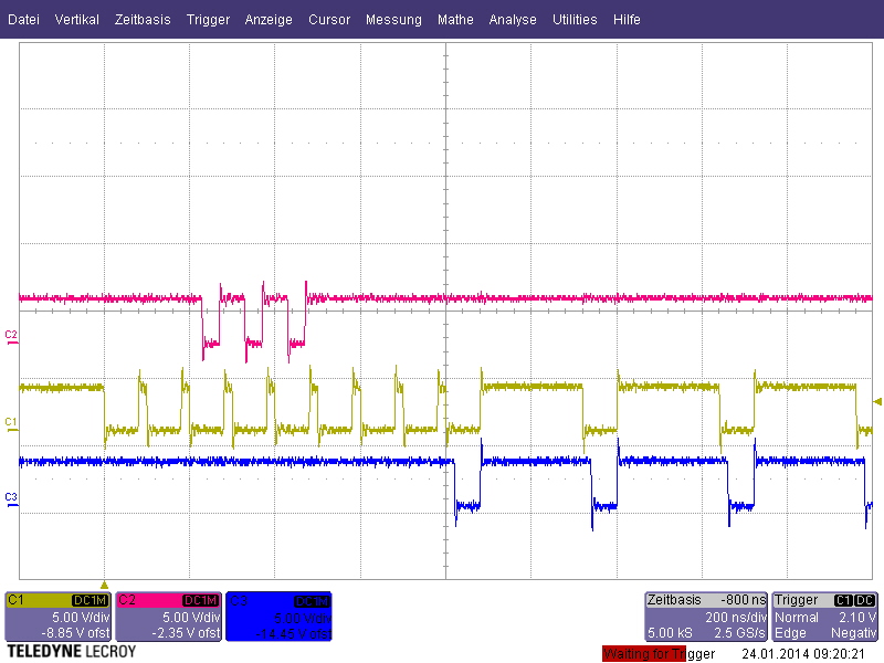
If I change the code to the following...

  //### Test
  *((volatile unsigned short *)(0x09000004))=0x0001;
  asm(" DMB");
  *((volatile unsigned short *)(0x09000006))=0x0002;
  asm(" DMB");
  *((volatile unsigned short *)(0x09000008))=0x0003;
  asm(" DMB");
  //### Test Ende

...I can see the expected number of low cycles of the chip select signal.

Does anyone from TI has an idea why this happens? Is this a bug within the GPMC module?

Thanks and best regards,
Patrick

  • Hi Patrick,
     
     
    "The Data Memory Barrier (DMB) acts as a memory barrier. It has slightly different behavior to DSB. The DMB instruction will ensure that any memory accesses before the DMB have completed before any memory access from instructions following the DMB instruction are performed."
  • Hi Biser,

    Attached I have two scope screenshots. One shows the Chip Select signal (channel C1, yellow) how it should be. First you can see the three write accesses with the WEn signal on channel C2 (red). The 4 following accesses are read access with OEn (Output Enable) signal on channel C3 (blue). This is how it should be. But I can only do this unsing the "DMB" instruction.


    The scond scope screenshot shows the write access without the "DMB" instructions. It clearly shows that the chip select signal goes low without a WEn or OEn signal activ.


    Can you please explain why the Chip Select signal goes low five times more than it should?

    Thanks.
    Patrick

  • What software are you using?

  • We use our own software. Developed on CCS V5.5 with TI compiler V5.0.5. No SYSBIOS. The code is as posted in the first post. The memory range is non-chachable, non-sharable, non-secure, execute never. It is a Dual Port RAM connected to GPMC with 16Bit databus.

  • I'm sorry, I cannot help on custom software. You have posted only the write accesses, and there are just too many initializations involved before them.

  • But maybe someone from TI can tell why the chip select signal can go low although WEn and OEn both stay high. And this in a configuration where normally for a write access the WEn signal goes low and for a read access the OEn signal goes low.

  • Hi,

    Any news on this topic?

  • Please double-check your MMU mappings.  I've seen issues very similar to this that were due to the GPMC mapping not being properly configured as device or strongly ordered.  If that's the case then you end up with speculative accesses to the memory.

  • Hi Brad,

    Thanks for this answer. Yes, the mapping for the Dual Port RAM is currently set to "Normal, non-shareable". In general what setting would you recommend for:

    a) External Flash M29W160EB (like the one on the AM335x ICE board)

    b) External Static RAM (like a Dual Port RAM on the AM335x ICE board (not populated))

    Would you use memory type "Device" or "Strongly Ordered"? We are new to the MMU topic and as far as I have seen there is no example in the StarterWare using an external flash or static RAM with MMU enabled. I have also read the ARM manuals about the MMU memory type attributes but for me it is not so clear which attribute to use in which case.

    Thanks for the support,
    Patrick

  • In both scenarios your GPMC configuration is the same.  The issue is not related to the GPMC, but rather to the way in which the ARM generates accesses.  Can you try out your accesses with the memory marked as device or strongly ordered just to verify that we're on the right path?  Your use case and requirements will play a large part in determining the proper type of memory.  Here are a few notes:

    • Normal -- this allows data to be cached, writes to be buffered, as well as speculative fetches of data and instructions.  You would have best performance in this case (more efficient bursting, caching, etc.) but at the expense of additional complexity in your software to ensure cache coherence between the two processors sharing the dual-port RAM.
    • Strongly ordered -- this disables caching, buffering, and speculative fetches.  This is extremely safe in terms of avoiding any potential ordering issues or coherence problems.
    • Device -- this is similar to strongly ordered in that it disables caching and speculative fetches.  It will however allow buffering of data.  This can have a nice performance improvement.  For example, if you're doing several back-to-back writes the CPU will "fire and forget" with device memory.  For strongly ordered you would incur a long CPU stall between each write, because the CPU would be stalled until the write actually landed in the external memory.

    So this is clearly going to be very use case dependent.  As a more general statement I think the "device" setting is a good compromise in terms of performance and programming simplicity for this type of scenario where you're sharing a RAM with some other processor!  For an external (single port) SRAM I would definitely mark that as "normal".  Due to the fact that you're sharing with something else you run into cache coherence considerations which is why you might consider "device".

    So in the case of an external flash you would need to make sure that some of the specific command sequences make it to the flash as expected.  It would be easiest to configure it as "device" for this purpose. I've seen customers do clever things such as logically ANDing two chip selects together to go to the external flash.  That way they could configure one chip select space as "device" for doing all the commands and they could configure a separate chip select space as "normal" for doing all the reads.  That also allowed them the flexibility to use async for the commands and sync for the data.

  • Hi Brad,

    That was for sure one of the best answers I got on the TI E2E so far. Thank you very much for taking the time to explain in detail. I'm sure this will help other users as well.
    As you have expected  in your first post, the problem was because of the memory type "normal". I have changed it to type "strongly ordered" and the problem was gone. Then I have also tried the type "device" and also the problem was solved but with a clear performance boost over the type "strongly ordered" (as you describe it in your second post).
    Your hint about logically ANDing two chip selects is pretty helpful and interesting. Last September we ran into exactly this problem with the flash. This time we solved the problem (writing command have been interrupted by reads) with the command "DMB". With your last post I now know why and how it works.

    Thanks a lot and best regards,
    Patrick

  • Glad I could help!  Thank you for reporting back your results and for verifying your answer in order to close the thread.