This thread has been locked.

If you have a related question, please click the "Ask a related question" button in the top right corner. The newly created question will be automatically linked to this question.

LAN8710A PHY on AM3359 through RMII2

Other Parts Discussed in Thread: AM3359

hi,everyone

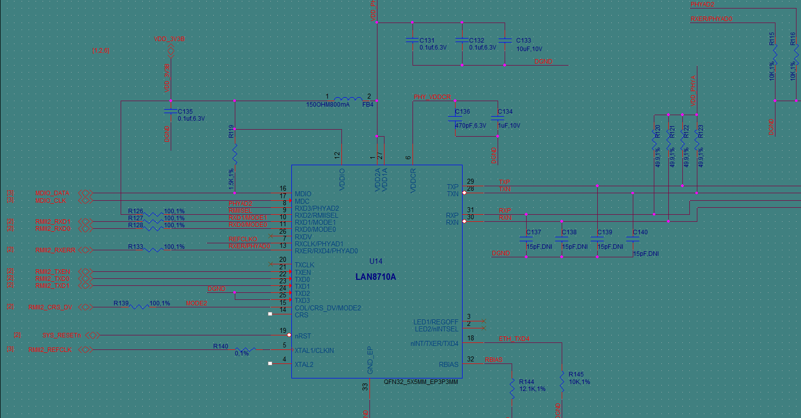
I use a LAN8710A PHY connect am3359 through RMII2 ,I used the SDK06.00.00 is latest version,

I adjust the configuration in uboot and provide a external low jitter 50 MHz RMII LVCMOS reference clock to both LAN8710a and AM335x.

First I configure the gmii_sel register is 0x75,then configure the pinmux

static struct module_pin_mux rmii2_pin_mux[] = {
{OFFSET(gpmc_a11), MODE(3) | RXACTIVE}, /* RMII2_RXD0 */
{OFFSET(gpmc_a10), MODE(3) | RXACTIVE}, /* RMII2_RXD1 */
{OFFSET(gpmc_wpn), MODE(3) | RXACTIVE}, /* RMII2_RXERR */
{OFFSET(gpmc_a0), MODE(3)}, /* RMII2_TXEN */
{OFFSET(gpmc_a5), MODE(3)}, /* RMII2_TXD0 */
{OFFSET(gpmc_a4), MODE(3)}, /* RMII2_TXD1 */
{OFFSET(gpmc_wait0), MODE(3) | RXACTIVE}, /* RMII2_CRS_DV */
{OFFSET(mii_col), MODE(1)}, /* RMII2_REFCLK */
{OFFSET(mdio_data), MODE(0) | RXACTIVE | PULLUP_EN},/* MDIO_DATA */
{OFFSET(mdio_clk), MODE(0) | PULLUP_EN}, /* MDIO_CLK */
{-1},
};

I pulldown the PHY address pin,configure the phy_id like this

static struct cpsw_slave_data cpsw_slaves[] = {
{
.slave_reg_ofs = 0x208,
.sliver_reg_ofs = 0xd80,
.phy_id = 1,
},
{
.slave_reg_ofs = 0x308,
.sliver_reg_ofs = 0xdc0,
.phy_id = 0,
},
};

then I execution dhcp in uboot  ,it appears that

U-Boot# dhcp
link up on port 0, speed 100, full duplex
BOOTP broadcast 1
BOOTP broadcast 2
BOOTP broadcast 3
BOOTP broadcast 4
BOOTP broadcast 5
BOOTP broadcast 6
BOOTP broadcast 7
BOOTP broadcast 8
BOOTP broadcast 9
BOOTP broadcast 10

Retry count exceeded; starting again
using musb-hdrc, OUT ep1out IN ep1in STATUS ep2in
MAC bc:6a:29:73:f6:90
HOST MAC de:ad:be:af:00:00
RNDIS ready
ERROR: The remote end did not respond in time.
at ether.c:2395/usb_eth_init()
link up on port 0, speed 100, full duplex

Did I miss a configuration step?Is there anything else that configure RMII2?


  • First you must have RXACTIVE on RMII_REFCLK. Second, do you have any other signal connected to RMII2_CRS_DV, like NAND R/B signal?

  • hi,Biser Gatchev-XID

    I did some modifications as you suggested

    but it still does not work.

    Do you mean that there may have pinmux conflict?  I checked two files:

    u-boot-2013.01.01-psp06.00.00.00/board/ti/am335x/board.c and mux.c .

    Is there any files I should checked for pinmux?

    Because of my negligence,the RMII2_CRS_DV signal   picked up fly line ,

    so it is longer than some of the other signal lines,what impact for the system work?

    thank you!

  • Ge,

    Are you sure the upstream BOOTP host is working? From the log you posted it appear that we can communicate well with our PHY, but that the remote host is not responding.

    As for your CRS_DV issue, it's possible that the mis-match on CRS_DV could cause the interface to fail. it would depend on several factors, with the mismatch delta being the most critical. Have you already run a timing analysis on the RMII interface? If not, post your RMII interface total signal lengths (all of them) and I'll take a look at it.

  • Hi,DK

    thank you for your answer;

    I rarely know the BOOTP ,how can I make sure it work?

    This is my signal lengths:

    MDIO_DATA  590.19 MIL

    MDIO_CLK    568.99 MIL

    RMII2_RXD1  993.59 MIL

    RMII2_RXD0  893.98 MIL

    RMII2_RXEER 889.86 MIL

    RMII2_TXD0  816.85 MIL

    RMII2_TXD1  845.54 MIL

    RMII2_TXEN 829.94 MIL

    RMII2_REFCLK  996 MIL

    RMII2_CRS_DV  5730 MIL (this signal line pick up some fly line )

    I am surprise that I chose rmii2 interface, why it was displayed “link up on port 0” in uboot .I think it should show “link up on  port 1”, is it?

  • Ge,

    Could you break down the RMII_REFCLK length? In other words, I need to know the clock source-to-MAC and clock source-to-PHY lengths.

    Thanks.

  • ok,DK

    I measured the length of their.

    The clock source-to-MAC lengths is 3870 MIL

    The clock source-to-PHY  lengths is 2938 MIL

  • I'm confused...where did the 996mils for RMII_REFCLK number come from in your earlier post?

  • Hi,DK

    I'm sorry I did not say it clearly.

    The day before yesterday I used AM3359 reference clock as the clock source output 50Mhz,but the PHY did not work.Then I knew I needed to provide a external low jitter 50 MHz RMII LVCMOS reference clock to both LAN8710A and AM3359.

    So I pick up a 50Mhz crystal through  fly line instead of the AM3359's clock .

    The 996mils is the RMII_REFCLK length from AM3359's pin to PHY's pin,and  it is not used now.

    The 3870mils is the length of clock source-to-mac being used now.

    The 2893mils is the length of clock source-to-phy being used now.

    Are there any problems for my clock signal length?

    Thank you!

  • I understand. I performed a quick analysis of your interface timing and I don't see a problem. Let's take a step back and look at more functional issues (like configuration)...

    Did you change the PADCONFIG for RMII_REFCLK to INPUT as suggested by Biser earlier in this thread?

    Did you configure the both the MAC (AM335x TRM section 14.5.7.2) and PHY (SMSC datasheet section 3.7.3) for RMII modes? Please provide the value of AM335x MACCONTROL register.

    Can you manually assign the interface an IP address, trying pinging an external address, and check CPSW_STATS (AM335x TRM section 14.5.4) to see if packet counters are incrementing? 

  • /*
     * board.c
     *
     * Board functions for TI AM335X based boards
     *
     * Copyright (C) 2011, Texas Instruments, Incorporated - http://www.ti.com/
     *
     * This program is free software; you can redistribute it and/or
     * modify it under the terms of the GNU General Public License as
     * published by the Free Software Foundation; either version 2 of
     * the License, or (at your option) any later version.
     *
     * This program is distributed in the hope that it will be useful,
     * but WITHOUT ANY WARRANTY; without even the implied warranty of
     * MERCHANTABILITY or FITNESS FOR A PARTICULAR /PURPOSE.  See the
     * GNU General Public License for more details.
     */
    
    #include <common.h>
    #include <errno.h>
    #include <spl.h>
    #include <asm/arch/cpu.h>
    #include <asm/arch/hardware.h>
    #include <asm/arch/omap.h>
    #include <asm/arch/ddr_defs.h>
    #include <asm/arch/clock.h>
    #include <asm/arch/gpio.h>
    #include <asm/arch/mmc_host_def.h>
    #include <asm/arch/sys_proto.h>
    #include <asm/io.h>
    #include <asm/emif.h>
    #include <asm/gpio.h>
    #include <i2c.h>
    #include <miiphy.h>
    #include <cpsw.h>
    #include "board.h"
    #include "pmic.h"
    #include "tps65217.h"
    
    DECLARE_GLOBAL_DATA_PTR;
    
    static struct wd_timer *wdtimer = (struct wd_timer *)WDT_BASE;
    #if defined(CONFIG_SPL_BUILD) || (CONFIG_NOR_BOOT)
    static struct uart_sys *uart_base = (struct uart_sys *)DEFAULT_UART_BASE;
    #endif
    
    /* MII mode defines */
    #define MII_MODE_ENABLE		0x0
    #define RGMII_MODE_ENABLE	0x3A
    #define RMII_MODE_ENABLE    0x77
    
    /* GPIO that controls power to DDR on EVM-SK */
    #define GPIO_DDR_VTT_EN		7
    
    static struct ctrl_dev *cdev = (struct ctrl_dev *)CTRL_DEVICE_BASE;
    
    static struct am335x_baseboard_id __attribute__((section (".data"))) header;
    
    static inline int board_is_bone(void)
    {
    	return !strncmp(header.name, "A335BONE", HDR_NAME_LEN);
    }
    
    static inline int board_is_bone_lt(void)
    {
    	return !strncmp(header.name, "A335BNLT", HDR_NAME_LEN);
    }
    
    static inline int board_is_evm_sk(void)
    {
    	return !strncmp("A335X_SK", header.name, HDR_NAME_LEN);
    }
    
    static inline int board_is_idk(void)
    {
    	return !strncmp(header.config, "SKU#02", 6);
    }
    
    static int __maybe_unused board_is_gp_evm(void)
    {
    	return !strncmp("A33515BB", header.name, 8);
    }
    
    int board_is_evm_15_or_later(void)
    {
    	return (!strncmp("A33515BB", header.name, 8) &&
    		strncmp("1.5", header.version, 3) <= 0);
    }
    
    /*
     * Read header information from EEPROM into global structure.
     */
    static int read_eeprom(void)
    {
    	/* Check if baseboard eeprom is available */
    	if (i2c_probe(CONFIG_SYS_I2C_EEPROM_ADDR)) {
    		puts("Could not probe the EEPROM; something fundamentally "
    			"wrong on the I2C bus.\n");
    		return -ENODEV;
    	}
    
    	/* read the eeprom using i2c */
    	if (i2c_read(CONFIG_SYS_I2C_EEPROM_ADDR, 0, 2, (uchar *)&header,
    							sizeof(header))) {
    		puts("Could not read the EEPROM; something fundamentally"
    			" wrong on the I2C bus.\n");
    		return -EIO;
    	}
    
    	if (header.magic != 0xEE3355AA) {
    		/*
    		 * read the eeprom using i2c again,
    		 * but use only a 1 byte address
    		 */
    		if (i2c_read(CONFIG_SYS_I2C_EEPROM_ADDR, 0, 1,
    					(uchar *)&header, sizeof(header))) {
    			puts("Could not read the EEPROM; something "
    				"fundamentally wrong on the I2C bus.\n");
    			return -EIO;
    		}
    
    		if (header.magic != 0xEE3355AA) {
    			printf("Incorrect magic number (0x%x) in EEPROM\n",
    					header.magic);
    			return -EINVAL;
    		}
    	}
    
    	return 0;
    }
    
    /* UART Defines */
    #if defined(CONFIG_SPL_BUILD) || defined(CONFIG_NOR_BOOT)
    /**
     * tps65217_reg_read() - Generic function that can read a TPS65217 register
     * @src_reg:          Source register address
     * @src_val:          Address of destination variable
     */
    
    unsigned char tps65217_reg_read(uchar src_reg, uchar *src_val)
    {
            if (i2c_read(TPS65217_CHIP_PM, src_reg, 1, src_val, 1))
                    return 1;
            return 0;
    }
    
    /**
     *  tps65217_reg_write() - Generic function that can write a TPS65217 PMIC
     *                         register or bit field regardless of protection
     *                         level.
     *
     *  @prot_level:        Register password protection.
     *                      use PROT_LEVEL_NONE, PROT_LEVEL_1, or PROT_LEVEL_2
     *  @dest_reg:          Register address to write.
     *  @dest_val:          Value to write.
     *  @mask:              Bit mask (8 bits) to be applied.  Function will only
     *                      change bits that are set in the bit mask.
     *
     *  @return:            0 for success, 1 for failure.
     */
    int tps65217_reg_write(uchar prot_level, uchar dest_reg,
            uchar dest_val, uchar mask)
    {
            uchar read_val;
            uchar xor_reg;
    
            /* if we are affecting only a bit field, read dest_reg and apply the mask */
            if (mask != MASK_ALL_BITS) {
                    if (i2c_read(TPS65217_CHIP_PM, dest_reg, 1, &read_val, 1))
                            return 1;
                    read_val &= (~mask);
                    read_val |= (dest_val & mask);
                    dest_val = read_val;
            }
    
            if (prot_level > 0) {
                    xor_reg = dest_reg ^ PASSWORD_UNLOCK;
                    if (i2c_write(TPS65217_CHIP_PM, PASSWORD, 1, &xor_reg, 1))
                            return 1;
            }
    
            if (i2c_write(TPS65217_CHIP_PM, dest_reg, 1, &dest_val, 1))
                    return 1;
    
            if (prot_level == PROT_LEVEL_2) {
                    if (i2c_write(TPS65217_CHIP_PM, PASSWORD, 1, &xor_reg, 1))
                            return 1;
    
                    if (i2c_write(TPS65217_CHIP_PM, dest_reg, 1, &dest_val, 1))
                            return 1;
            }
    
            return 0;
    }
    
    int tps65217_voltage_update(unsigned char dc_cntrl_reg, unsigned char volt_sel)
    {
            if ((dc_cntrl_reg != DEFDCDC1) && (dc_cntrl_reg != DEFDCDC2)
                    && (dc_cntrl_reg != DEFDCDC3))
                    return 1;
    
            /* set voltage level */
            if (tps65217_reg_write(PROT_LEVEL_2, dc_cntrl_reg, volt_sel, MASK_ALL_BITS))
                    return 1;
    
            /* set GO bit to initiate voltage transition */
            if (tps65217_reg_write(PROT_LEVEL_2, DEFSLEW, DCDC_GO, DCDC_GO))
                    return 1;
    
            return 0;
    }
    
    /*
     * voltage switching for MPU frequency switching.
     * @module = mpu - 0, core - 1
     * @vddx_op_vol_sel = vdd voltage to set
     */
    
    #define MPU     0
    #define CORE    1
    
    int voltage_update(unsigned int module, unsigned char vddx_op_vol_sel)
    {
            uchar buf[4];
            unsigned int reg_offset;
    
            if(module == MPU)
                    reg_offset = PMIC_VDD1_OP_REG;
            else
                    reg_offset = PMIC_VDD2_OP_REG;
    
            /* Select VDDx OP   */
            if (i2c_read(PMIC_CTRL_I2C_ADDR, reg_offset, 1, buf, 1))
                    return 1;
    
            buf[0] &= ~PMIC_OP_REG_CMD_MASK;
    
            if (i2c_write(PMIC_CTRL_I2C_ADDR, reg_offset, 1, buf, 1))
                    return 1;
    
            /* Configure VDDx OP  Voltage */
            if (i2c_read(PMIC_CTRL_I2C_ADDR, reg_offset, 1, buf, 1))
                    return 1;
    
            buf[0] &= ~PMIC_OP_REG_SEL_MASK;
            buf[0] |= vddx_op_vol_sel;
    
            if (i2c_write(PMIC_CTRL_I2C_ADDR, reg_offset, 1, buf, 1))
                    return 1;
    
            if (i2c_read(PMIC_CTRL_I2C_ADDR, reg_offset, 1, buf, 1))
                    return 1;
    
            if ((buf[0] & PMIC_OP_REG_SEL_MASK ) != vddx_op_vol_sel)
                    return 1;
    
            return 0;
    }
    
    #define UART_RESET		(0x1 << 1)
    #define UART_CLK_RUNNING_MASK	0x1
    #define UART_SMART_IDLE_EN	(0x1 << 0x3)
    
    static void rtc32k_enable(void)
    {
    	struct rtc_regs *rtc = (struct rtc_regs *)AM335X_RTC_BASE;
    
    	/*
    	 * Unlock the RTC's registers.  For more details please see the
    	 * RTC_SS section of the TRM.  In order to unlock we need to
    	 * write these specific values (keys) in this order.
    	 */
    	writel(0x83e70b13, &rtc->kick0r);
    	writel(0x95a4f1e0, &rtc->kick1r);
    
    	/* Enable the RTC 32K OSC by setting bits 3 and 6. */
    	writel((1 << 3) | (1 << 6), &rtc->osc);
    }
    
    static const struct ddr_data ddr2_data = {
    	.datardsratio0 = ((MT47H128M16RT25E_RD_DQS<<30) |
    			  (MT47H128M16RT25E_RD_DQS<<20) |
    			  (MT47H128M16RT25E_RD_DQS<<10) |
    			  (MT47H128M16RT25E_RD_DQS<<0)),
    	.datawdsratio0 = ((MT47H128M16RT25E_WR_DQS<<30) |
    			  (MT47H128M16RT25E_WR_DQS<<20) |
    			  (MT47H128M16RT25E_WR_DQS<<10) |
    			  (MT47H128M16RT25E_WR_DQS<<0)),
    	.datawiratio0 = ((MT47H128M16RT25E_PHY_WRLVL<<30) |
    			 (MT47H128M16RT25E_PHY_WRLVL<<20) |
    			 (MT47H128M16RT25E_PHY_WRLVL<<10) |
    			 (MT47H128M16RT25E_PHY_WRLVL<<0)),
    	.datagiratio0 = ((MT47H128M16RT25E_PHY_GATELVL<<30) |
    			 (MT47H128M16RT25E_PHY_GATELVL<<20) |
    			 (MT47H128M16RT25E_PHY_GATELVL<<10) |
    			 (MT47H128M16RT25E_PHY_GATELVL<<0)),
    	.datafwsratio0 = ((MT47H128M16RT25E_PHY_FIFO_WE<<30) |
    			  (MT47H128M16RT25E_PHY_FIFO_WE<<20) |
    			  (MT47H128M16RT25E_PHY_FIFO_WE<<10) |
    			  (MT47H128M16RT25E_PHY_FIFO_WE<<0)),
    	.datawrsratio0 = ((MT47H128M16RT25E_PHY_WR_DATA<<30) |
    			  (MT47H128M16RT25E_PHY_WR_DATA<<20) |
    			  (MT47H128M16RT25E_PHY_WR_DATA<<10) |
    			  (MT47H128M16RT25E_PHY_WR_DATA<<0)),
    	.datauserank0delay = MT47H128M16RT25E_PHY_RANK0_DELAY,
    	.datadldiff0 = PHY_DLL_LOCK_DIFF,
    };
    
    static const struct cmd_control ddr2_cmd_ctrl_data = {
    	.cmd0csratio = MT47H128M16RT25E_RATIO,
    	.cmd0dldiff = MT47H128M16RT25E_DLL_LOCK_DIFF,
    	.cmd0iclkout = MT47H128M16RT25E_INVERT_CLKOUT,
    
    	.cmd1csratio = MT47H128M16RT25E_RATIO,
    	.cmd1dldiff = MT47H128M16RT25E_DLL_LOCK_DIFF,
    	.cmd1iclkout = MT47H128M16RT25E_INVERT_CLKOUT,
    
    	.cmd2csratio = MT47H128M16RT25E_RATIO,
    	.cmd2dldiff = MT47H128M16RT25E_DLL_LOCK_DIFF,
    	.cmd2iclkout = MT47H128M16RT25E_INVERT_CLKOUT,
    };
    
    static const struct emif_regs ddr2_emif_reg_data = {
    	.sdram_config = MT47H128M16RT25E_EMIF_SDCFG,
    	.ref_ctrl = MT47H128M16RT25E_EMIF_SDREF,
    	.sdram_tim1 = MT47H128M16RT25E_EMIF_TIM1,
    	.sdram_tim2 = MT47H128M16RT25E_EMIF_TIM2,
    	.sdram_tim3 = MT47H128M16RT25E_EMIF_TIM3,
    	.emif_ddr_phy_ctlr_1 = MT47H128M16RT25E_EMIF_READ_LATENCY,
    };
    
    static const struct ddr_data ddr3_data = {
    	.datardsratio0 = MT41J128MJT125_RD_DQS,
    	.datawdsratio0 = MT41J128MJT125_WR_DQS,
    	.datafwsratio0 = MT41J128MJT125_PHY_FIFO_WE,
    	.datawrsratio0 = MT41J128MJT125_PHY_WR_DATA,
    	.datadldiff0 = PHY_DLL_LOCK_DIFF,
    };
    
    static const struct ddr_data ddr3_beagleblack_data = {
    	.datardsratio0 = MT41K256M16HA125E_RD_DQS,
     	.datawdsratio0 = MT41K256M16HA125E_WR_DQS,
    	.datafwsratio0 = MT41K256M16HA125E_PHY_FIFO_WE,
    	.datawrsratio0 = MT41K256M16HA125E_PHY_WR_DATA,
    	.datadldiff0 = PHY_DLL_LOCK_DIFF,
    };
    
    static const struct ddr_data ddr3_evm_data = {
    	.datardsratio0 = MT41J512M8RH125_RD_DQS,
    	.datawdsratio0 = MT41J512M8RH125_WR_DQS,
    	.datafwsratio0 = MT41J512M8RH125_PHY_FIFO_WE,
    	.datawrsratio0 = MT41J512M8RH125_PHY_WR_DATA,
    	.datadldiff0 = PHY_DLL_LOCK_DIFF,
    };
    
    static const struct cmd_control ddr3_cmd_ctrl_data = {
    	.cmd0csratio = MT41J128MJT125_RATIO,
    	.cmd0dldiff = MT41J128MJT125_DLL_LOCK_DIFF,
    	.cmd0iclkout = MT41J128MJT125_INVERT_CLKOUT,
    
    	.cmd1csratio = MT41J128MJT125_RATIO,
    	.cmd1dldiff = MT41J128MJT125_DLL_LOCK_DIFF,
    	.cmd1iclkout = MT41J128MJT125_INVERT_CLKOUT,
    
    	.cmd2csratio = MT41J128MJT125_RATIO,
    	.cmd2dldiff = MT41J128MJT125_DLL_LOCK_DIFF,
    	.cmd2iclkout = MT41J128MJT125_INVERT_CLKOUT,
    };
    
    static const struct cmd_control ddr3_beagleblack_cmd_ctrl_data = {
    	.cmd0csratio = MT41K256M16HA125E_RATIO,
    	.cmd0dldiff = MT41K256M16HA125E_DLL_LOCK_DIFF,
    	.cmd0iclkout = MT41K256M16HA125E_INVERT_CLKOUT,
    
    	.cmd1csratio = MT41K256M16HA125E_RATIO,
    	.cmd1dldiff = MT41K256M16HA125E_DLL_LOCK_DIFF,
    	.cmd1iclkout = MT41K256M16HA125E_INVERT_CLKOUT,
    
    	.cmd2csratio = MT41K256M16HA125E_RATIO,
    	.cmd2dldiff = MT41K256M16HA125E_DLL_LOCK_DIFF,
    	.cmd2iclkout = MT41K256M16HA125E_INVERT_CLKOUT,
    };
    
    static const struct cmd_control ddr3_evm_cmd_ctrl_data = {
    	.cmd0csratio = MT41J512M8RH125_RATIO,
    	.cmd0dldiff = MT41J512M8RH125_DLL_LOCK_DIFF,
    	.cmd0iclkout = MT41J512M8RH125_INVERT_CLKOUT,
    
    	.cmd1csratio = MT41J512M8RH125_RATIO,
    	.cmd1dldiff = MT41J512M8RH125_DLL_LOCK_DIFF,
    	.cmd1iclkout = MT41J512M8RH125_INVERT_CLKOUT,
    
    	.cmd2csratio = MT41J512M8RH125_RATIO,
    	.cmd2dldiff = MT41J512M8RH125_DLL_LOCK_DIFF,
    	.cmd2iclkout = MT41J512M8RH125_INVERT_CLKOUT,
    };
    
    static struct emif_regs ddr3_emif_reg_data = {
    	.sdram_config = MT41J128MJT125_EMIF_SDCFG,
    	.ref_ctrl = MT41J128MJT125_EMIF_SDREF,
    	.sdram_tim1 = MT41J128MJT125_EMIF_TIM1,
    	.sdram_tim2 = MT41J128MJT125_EMIF_TIM2,
    	.sdram_tim3 = MT41J128MJT125_EMIF_TIM3,
    	.zq_config = MT41J128MJT125_ZQ_CFG,
    	.emif_ddr_phy_ctlr_1 = MT41J128MJT125_EMIF_READ_LATENCY |
    				PHY_EN_DYN_PWRDN,
    };
    
    static struct emif_regs ddr3_beagleblack_emif_reg_data = {
    	.sdram_config = MT41K256M16HA125E_EMIF_SDCFG,
    	.ref_ctrl = MT41K256M16HA125E_EMIF_SDREF,
    	.sdram_tim1 = MT41K256M16HA125E_EMIF_TIM1,
    	.sdram_tim2 = MT41K256M16HA125E_EMIF_TIM2,
    	.sdram_tim3 = MT41K256M16HA125E_EMIF_TIM3,
    	.zq_config = MT41K256M16HA125E_ZQ_CFG,
    	.emif_ddr_phy_ctlr_1 = MT41K256M16HA125E_EMIF_READ_LATENCY |
    				PHY_EN_DYN_PWRDN,
    };
    
    static struct emif_regs ddr3_evm_emif_reg_data = {
    	.sdram_config = MT41J512M8RH125_EMIF_SDCFG,
    	.ref_ctrl = MT41J512M8RH125_EMIF_SDREF,
    	.sdram_tim1 = MT41J512M8RH125_EMIF_TIM1,
    	.sdram_tim2 = MT41J512M8RH125_EMIF_TIM2,
    	.sdram_tim3 = MT41J512M8RH125_EMIF_TIM3,
    	.zq_config = MT41J512M8RH125_ZQ_CFG,
    	.emif_ddr_phy_ctlr_1 = MT41J512M8RH125_EMIF_READ_LATENCY |
    				PHY_EN_DYN_PWRDN,
    };
    
    void am33xx_spl_board_init(void)
    {
    	int mpu_vdd, mpu_pll, sil_rev;
    
    	/* Assume PG 1.0 */
    	mpu_pll = MPUPLL_M_720;
    
    	sil_rev = readl(&cdev->deviceid) >> 28;
    	if (sil_rev == 1)
    		/* PG 2.0, efuse may not be set. */
    		mpu_pll = MPUPLL_M_800;
    	else if (sil_rev >= 2) {
    		/* Check what the efuse says our max speed is. */
    		int efuse_arm_mpu_max_freq;
    		efuse_arm_mpu_max_freq = readl(&cdev->efuse_sma);
    		if ((efuse_arm_mpu_max_freq & DEVICE_ID_MASK) ==
    				AM335X_ZCZ_1000)
    			mpu_pll = MPUPLL_M_1000;
    		else if ((efuse_arm_mpu_max_freq & DEVICE_ID_MASK) ==
    				AM335X_ZCZ_800)
    			mpu_pll = MPUPLL_M_800;
    	}
    
    	/*
    	 * HACK: PG 2.0 should have max of 800MHz but Beaglebone Black
    	 * can work at 1GHz.
    	 */
    	if (board_is_bone_lt())
    		mpu_pll = MPUPLL_M_1000;
    
    	if (board_is_bone() || board_is_bone_lt()) {
    		/* BeagleBone PMIC Code */
    		uchar pmic_status_reg;
    		int usb_cur_lim;
    
    		/* Only perform PMIC configurations if board rev > A1 */
    		if (board_is_bone() && !strncmp(header.version, "00A1", 4))
    			return;
    
    		if (i2c_probe(TPS65217_CHIP_PM))
    			return;
    
    		if (tps65217_reg_read(STATUS, &pmic_status_reg))
    			return;
    
    		/*
    		 * Increase USB current limit to 1300mA or 1800mA and set
    		 * the MPU voltage controller as needed.
    		 */
    		if (mpu_pll == MPUPLL_M_1000) {
    			usb_cur_lim = USB_INPUT_CUR_LIMIT_1800MA;
    			mpu_vdd = DCDC_VOLT_SEL_1325MV;
    		} else {
    			usb_cur_lim = USB_INPUT_CUR_LIMIT_1300MA;
    			mpu_vdd = DCDC_VOLT_SEL_1275MV;
    		}
    
    		if (tps65217_reg_write(PROT_LEVEL_NONE, POWER_PATH,
    				       usb_cur_lim, USB_INPUT_CUR_LIMIT_MASK))
    			printf("tps65217_reg_write failure\n");
    
    		/* Set DCDC3 (CORE) voltage to 1.125V */
    		if (tps65217_voltage_update(DEFDCDC3, DCDC_VOLT_SEL_1125MV)) {
    			printf("tps65217_voltage_update failure\n");
    			return;
    		}
    
    		/* Set CORE Frequency to what we detected */
    		core_pll_config(OPP_100);
    
    		/* Set DCDC2 (MPU) voltage to 1.275V */
    		if (tps65217_voltage_update(DEFDCDC2, mpu_vdd)) {
    			printf("tps65217_voltage_update failure\n");
    			return;
    		}
    
    		/* Set MPU Frequency to what we detected */
    		mpu_pll_config(mpu_pll);
    
    		/*
    		 * Set LDO3, LDO4 output voltage to 3.3V for Beaglebone.
    		 * Set LDO3 to 1.8V and LDO4 to 3.3V for Beaglebone Black.
    		 */
    		if (board_is_bone()) {
    			if (tps65217_reg_write(PROT_LEVEL_2, DEFLS1,
    				       LDO_VOLTAGE_OUT_3_3, LDO_MASK))
    				printf("tps65217_reg_write failure\n");
    		} else {
    			if (tps65217_reg_write(PROT_LEVEL_2, DEFLS1,
    				       LDO_VOLTAGE_OUT_1_8, LDO_MASK))
    				printf("tps65217_reg_write failure\n");
    		}
    
    		if (tps65217_reg_write(PROT_LEVEL_2, DEFLS2,
    				       LDO_VOLTAGE_OUT_3_3, LDO_MASK))
    			printf("tps65217_reg_write failure\n");
    
    		/* Only Beaglebone needs the AC power, not Beaglebone Black */
    		if (board_is_bone() &&
    				 !(pmic_status_reg & PWR_SRC_AC_BITMASK)) {
    			printf("No AC power, disabling frequency switch\n");
    			return;
    		}
    	} else {
    		uchar buf[4];
    
    		/*
    		 * The GP EVM, IDK and EVM SK use a TPS65910 PMIC.  For all
    		 * MPU frequencies we support we use a CORE voltage of
    		 * 1.1375V.  For 1GHz we need to use an MPU voltage of
    		 * 1.3250V and for 720MHz or 800MHz we use 1.2625V.
    		 */
    		if (i2c_probe(PMIC_CTRL_I2C_ADDR))
    			return;
    
    		/* VDD1/2 voltage selection register access by control i/f */
    		if (i2c_read(PMIC_CTRL_I2C_ADDR, PMIC_DEVCTRL_REG, 1, buf, 1))
    			return;
    
    		buf[0] |= PMIC_DEVCTRL_REG_SR_CTL_I2C_SEL_CTL_I2C;
    
    		if (i2c_write(PMIC_CTRL_I2C_ADDR, PMIC_DEVCTRL_REG, 1, buf, 1))
    			return;
    
    		/*
    		 * Unless we're running at 1GHz we use thesame VDD for
    		 * all other frequencies we switch to (currently 720MHz,
    		 * 800MHz or 1GHz).
    		 */
    		if (mpu_pll == MPUPLL_M_1000)
    			mpu_vdd = PMIC_OP_REG_SEL_1_3_2_5;
    		else
    			mpu_vdd = PMIC_OP_REG_SEL_1_2_6;
    
    		if (!voltage_update(CORE, PMIC_OP_REG_SEL_1_1_3))
    			core_pll_config(OPP_100);
    		if (!voltage_update(MPU, mpu_vdd))
    			mpu_pll_config(mpu_pll);
    	}
    }
    #endif
    
    /*
     * early system init of muxing and clocks.
     */
    void s_init(void)
    {
    	__maybe_unused struct am335x_baseboard_id header;
    #ifdef CONFIG_NOR_BOOT
    	asm("stmfd      sp!, {r2 - r4}");
    	asm("movw       r4, #0x8A4");
    	asm("movw       r3, #0x44E1");
    	asm("orr        r4, r4, r3, lsl #16");
    	asm("mov        r2, #9");
    	asm("mov        r3, #8");
    	asm("gpmc_mux:  str     r2, [r4], #4");
    	asm("subs       r3, r3, #1");
    	asm("bne        gpmc_mux");
    	asm("ldmfd      sp!, {r2 - r4}");
    #endif
    
    	/* WDT1 is already running when the bootloader gets control
    	 * Disable it to avoid "random" resets
    	 */
    	writel(0xAAAA, &wdtimer->wdtwspr);
    	while (readl(&wdtimer->wdtwwps) != 0x0)
    		;
    	writel(0x5555, &wdtimer->wdtwspr);
    	while (readl(&wdtimer->wdtwwps) != 0x0)
    		;
    
    #if defined(CONFIG_SPL_BUILD) || defined(CONFIG_NOR_BOOT)
    	/* Setup the PLLs and the clocks for the peripherals */
    	pll_init();
    
    	/* Enable RTC32K clock */
    	rtc32k_enable();
    
    	/* UART softreset */
    	u32 regVal;
    
    #ifdef CONFIG_SERIAL1
    	enable_uart0_pin_mux();
    #endif /* CONFIG_SERIAL1 */
    #ifdef CONFIG_SERIAL2
    	enable_uart1_pin_mux();
    #endif /* CONFIG_SERIAL2 */
    #ifdef CONFIG_SERIAL3
    	enable_uart2_pin_mux();
    #endif /* CONFIG_SERIAL3 */
    #ifdef CONFIG_SERIAL4
    	enable_uart3_pin_mux();
    #endif /* CONFIG_SERIAL4 */
    #ifdef CONFIG_SERIAL5
    	//enable_uart4_pin_mux();
    #endif /* CONFIG_SERIAL5 */
    #ifdef CONFIG_SERIAL6
    	enable_uart5_pin_mux();
    #endif /* CONFIG_SERIAL6 */
    
    	regVal = readl(&uart_base->uartsyscfg);
    	regVal |= UART_RESET;
    	writel(regVal, &uart_base->uartsyscfg);
    	while ((readl(&uart_base->uartsyssts) &
    		UART_CLK_RUNNING_MASK) != UART_CLK_RUNNING_MASK)
    		;
    
    	/* Disable smart idle */
    	regVal = readl(&uart_base->uartsyscfg);
    	regVal |= UART_SMART_IDLE_EN;
    	writel(regVal, &uart_base->uartsyscfg);
    
    #if defined(CONFIG_NOR_BOOT)
    	gd = (gd_t *) ((CONFIG_SYS_INIT_SP_ADDR) & ~0x07);
    	gd->baudrate = CONFIG_BAUDRATE;
    	serial_init();
    	gd->have_console = 1;
    #else
    	gd = &gdata;
    
    	preloader_console_init();
    #endif
    
    	/* Initalize the board header */
    	enable_i2c0_pin_mux();
    	i2c_init(CONFIG_SYS_I2C_SPEED, CONFIG_SYS_I2C_SLAVE);
    #ifndef CONFIG_NOR_BOOT
    	if (read_eeprom() < 0)
    		puts("Could not get board ID.\n");
    #endif
    
    	/* Check if baseboard eeprom is available */
    	if (i2c_probe(CONFIG_SYS_I2C_EEPROM_ADDR)) {
    		puts("Could not probe the EEPROM; something fundamentally "
    			"wrong on the I2C bus.\n");
    	}
    
    	/* read the eeprom using i2c */
    	if (i2c_read(CONFIG_SYS_I2C_EEPROM_ADDR, 0, 2, (uchar *)&header,
    							sizeof(header))) {
    		puts("Could not read the EEPROM; something fundamentally"
    			" wrong on the I2C bus.\n");
    	}
    
    	if (header.magic != 0xEE3355AA) {
    		/*
    		 * read the eeprom using i2c again,
    		 * but use only a 1 byte address
    		 */
    		if (i2c_read(CONFIG_SYS_I2C_EEPROM_ADDR, 0, 1,
    					(uchar *)&header, sizeof(header))) {
    			puts("Could not read the EEPROM; something "
    				"fundamentally wrong on the I2C bus.\n");
    			hang();
    		}
    
    		if (header.magic != 0xEE3355AA) {
    			printf("Incorrect magic number (0x%x) in EEPROM\n",
    					header.magic);
    			hang();
    		}
    	}
    
    	enable_board_pin_mux(&header);
    	if (!strncmp("A335X_SK", header.name, HDR_NAME_LEN)) {
    		/*
    		 * EVM SK 1.2A and later use gpio0_7 to enable DDR3.
    		 * This is safe enough to do on older revs.
    		 */
    		gpio_request(GPIO_DDR_VTT_EN, "ddr_vtt_en");
    		gpio_direction_output(GPIO_DDR_VTT_EN, 1);
    	}
    
    #ifdef CONFIG_NOR_BOOT
    	am33xx_spl_board_init();
    #endif
    
    	if (!strncmp("A335X_SK", header.name, HDR_NAME_LEN))
    		config_ddr(303, MT41J128MJT125_IOCTRL_VALUE, &ddr3_data,
    			   &ddr3_cmd_ctrl_data, &ddr3_emif_reg_data);
    	else if  (!strncmp("A335BNLT", header.name, 8))
    		config_ddr(400, MT41K256M16HA125E_IOCTRL_VALUE,
    			   &ddr3_beagleblack_data,
    			   &ddr3_beagleblack_cmd_ctrl_data,
    			   &ddr3_beagleblack_emif_reg_data);
    	else if (!strncmp("A33515BB", header.name, 8) &&
    				strncmp("1.5", header.version, 3) <= 0)
    		config_ddr(303, MT41J512M8RH125_IOCTRL_VALUE, &ddr3_evm_data,
    			   &ddr3_evm_cmd_ctrl_data, &ddr3_evm_emif_reg_data);
    	else
    		config_ddr(266, MT47H128M16RT25E_IOCTRL_VALUE, &ddr2_data,
    			   &ddr2_cmd_ctrl_data, &ddr2_emif_reg_data);
    #endif
    }
    
    /*
     * Basic board specific setup.  Pinmux has been handled already.
     */
    int board_init(void)
    {
    	i2c_init(CONFIG_SYS_I2C_SPEED, CONFIG_SYS_I2C_SLAVE);
    	if (read_eeprom() < 0)
    		puts("Could not get board ID.\n");
    
    	gd->bd->bi_boot_params = PHYS_DRAM_1 + 0x100;
    
    	gpmc_init();
    
    	return 0;
    }
    
    #ifdef CONFIG_BOARD_LATE_INIT
    int board_late_init(void)
    {
    #ifdef CONFIG_ENV_VARS_UBOOT_RUNTIME_CONFIG
    	char safe_string[HDR_NAME_LEN + 1];
    
    	/* Now set variables based on the header. */
    	strncpy(safe_string, (char *)header.name, sizeof(header.name));
    	safe_string[sizeof(header.name)] = 0;
    	setenv("board_name", safe_string);
    
    	strncpy(safe_string, (char *)header.version, sizeof(header.version));
    	safe_string[sizeof(header.version)] = 0;
    	setenv("board_rev", safe_string);
    #endif
    
    	return 0;
    }
    #endif
    
    #if (defined(CONFIG_DRIVER_TI_CPSW) && !defined(CONFIG_SPL_BUILD)) || \
    	(defined(CONFIG_SPL_ETH_SUPPORT) && defined(CONFIG_SPL_BUILD))
    static void cpsw_control(int enabled)
    {
    	/* VTP can be added here */
    
    	return;
    }
    
    static struct cpsw_slave_data cpsw_slaves[] = {
    	{
    		.slave_reg_ofs	= 0x208,
    		.sliver_reg_ofs	= 0xd80,
    		.phy_id		= 1,
    	},
    	{
    		.slave_reg_ofs	= 0x308,
    		.sliver_reg_ofs	= 0xdc0,
    		.phy_id		= 0,
    	},
    };
    
    static struct cpsw_platform_data cpsw_data = {
    	.mdio_base		= AM335X_CPSW_MDIO_BASE,
    	.cpsw_base		= AM335X_CPSW_BASE,
    	.mdio_div		= 0xff,
    	.channels		= 8,
    	.cpdma_reg_ofs		= 0x800,
    	.slaves			= 1,
    	.slave_data		= cpsw_slaves,
    	.ale_reg_ofs		= 0xd00,
    	.ale_entries		= 1024,
    	.host_port_reg_ofs	= 0x108,
    	.hw_stats_reg_ofs	= 0x900,
    	.mac_control		= (1 << 5),
    	.control		= cpsw_control,
    	.host_port_num		= 0,
    	.version		= CPSW_CTRL_VERSION_2,
    };
    #endif
    
    #if defined(CONFIG_DRIVER_TI_CPSW) || \
    	(defined(CONFIG_USB_ETHER) && defined(CONFIG_MUSB_GADGET))
    int board_eth_init(bd_t *bis)
    {
    	int rv, n = 0;
    	uint8_t mac_addr[6];
    	uint32_t mac_hi, mac_lo;
    
    	/* try reading mac address from efuse */
    	mac_lo = readl(&cdev->macid0l);
    	mac_hi = readl(&cdev->macid0h);
    	mac_addr[0] = mac_hi & 0xFF;
    	mac_addr[1] = (mac_hi & 0xFF00) >> 8;
    	mac_addr[2] = (mac_hi & 0xFF0000) >> 16;
    	mac_addr[3] = (mac_hi & 0xFF000000) >> 24;
    	mac_addr[4] = mac_lo & 0xFF;
    	mac_addr[5] = (mac_lo & 0xFF00) >> 8;
    
    #if (defined(CONFIG_DRIVER_TI_CPSW) && !defined(CONFIG_SPL_BUILD)) || \
    	(defined(CONFIG_SPL_ETH_SUPPORT) && defined(CONFIG_SPL_BUILD))
    	if (!getenv("ethaddr")) {
    		printf("<ethaddr> not set. Validating first E-fuse MAC\n");
    
    		if (is_valid_ether_addr(mac_addr))
    			eth_setenv_enetaddr("ethaddr", mac_addr);
    	}
    
    	if (board_is_bone() || board_is_bone_lt() || board_is_idk()) {
    		writel(RMII_MODE_ENABLE, &cdev->miisel);
    		cpsw_slaves[0].phy_if = cpsw_slaves[1].phy_if =
    				PHY_INTERFACE_MODE_RMII;
    		printf("RMII MODE instable");
    	} else {
    		writel(RGMII_MODE_ENABLE, &cdev->miisel);
    		cpsw_slaves[0].phy_if = cpsw_slaves[1].phy_if =
    				PHY_INTERFACE_MODE_RGMII;
    		printf("RGMII MODE instable");
    	}
    
    	rv = cpsw_register(&cpsw_data);
    	if (rv < 0)
    		printf("Error %d registering CPSW switch\n", rv);
    	else
    		n += rv;
    
    	/*
    	 *
    	 * CPSW RGMII Internal Delay Mode is not supported in all PVT
    	 * operating points.  So we must set the TX clock delay feature
    	 * in the AR8051 PHY.  Since we only support a single ethernet
    	 * device in U-Boot, we only do this for the first instance.
    	 */
    #define AR8051_PHY_DEBUG_ADDR_REG	0x1d
    #define AR8051_PHY_DEBUG_DATA_REG	0x1e
    #define AR8051_DEBUG_RGMII_CLK_DLY_REG	0x5
    #define AR8051_RGMII_TX_CLK_DLY		0x100
    
    	if (board_is_evm_sk() || board_is_gp_evm()) {
    		const char *devname;
    		devname = miiphy_get_current_dev();
    
    		miiphy_write(devname, 0x0, AR8051_PHY_DEBUG_ADDR_REG,
    				AR8051_DEBUG_RGMII_CLK_DLY_REG);
    		miiphy_write(devname, 0x0, AR8051_PHY_DEBUG_DATA_REG,
    				AR8051_RGMII_TX_CLK_DLY);
    	}
    #endif
    #if defined(CONFIG_USB_ETHER) && \
    	(!defined(CONFIG_SPL_BUILD) || defined(CONFIG_SPL_USBETH_SUPPORT))
    	if (is_valid_ether_addr(mac_addr))
    		eth_setenv_enetaddr("usbnet_devaddr", mac_addr);
    
    	rv = usb_eth_initialize(bis);
    	if (rv < 0)
    		printf("Error %d registering USB_ETHER\n", rv);
    	else
    		n += rv;
    #endif
    	return n;
    }
    #endif
    
    /*
     * mux.c
     *
     * Copyright (C) 2011 Texas Instruments Incorporated - http://www.ti.com/
     *
     * This program is free software; you can redistribute it and/or
     * modify it under the terms of the GNU General Public License as
     * published by the Free Software Foundation version 2.
     *
     * This program is distributed "as is" WITHOUT ANY WARRANTY of any
     * kind, whether express or implied; without even the implied warranty
     * of MERCHANTABILITY or FITNESS FOR A PARTICULAR PURPOSE. See the
     * GNU General Public License for more details.
     */
    
    #include <common.h>
    #include <asm/arch/sys_proto.h>
    #include <asm/arch/hardware.h>
    #include <asm/arch/mux.h>
    #include <asm/io.h>
    #include <i2c.h>
    #include "board.h"
    
    static struct module_pin_mux uart0_pin_mux[] = {
    	{OFFSET(uart0_rxd), (MODE(0) | PULLUP_EN | RXACTIVE)},	/* UART0_RXD */
    	{OFFSET(uart0_txd), (MODE(0) | PULLUDEN)},		/* UART0_TXD */
    	{-1},
    };
    
    static struct module_pin_mux uart1_pin_mux[] = {
    	{OFFSET(uart1_rxd), (MODE(0) | PULLUP_EN | RXACTIVE)},	/* UART1_RXD */
    	{OFFSET(uart1_txd), (MODE(0) | PULLUDEN)},		/* UART1_TXD */
    	{-1},
    };
    
    static struct module_pin_mux uart2_pin_mux[] = {
    	{OFFSET(spi0_sclk), (MODE(1) | PULLUP_EN | RXACTIVE)},	/* UART2_RXD */
    	{OFFSET(spi0_d0), (MODE(1) | PULLUDEN)},		/* UART2_TXD */
    	{-1},
    };
    
    static struct module_pin_mux uart3_pin_mux[] = {
    	{OFFSET(spi0_cs1), (MODE(1) | PULLUP_EN | RXACTIVE)},	/* UART3_RXD */
    	{OFFSET(ecap0_in_pwm0_out), (MODE(1) | PULLUDEN)},	/* UART3_TXD */
    	{-1},
    };
    
    static struct module_pin_mux uart4_pin_mux[] = {
    	{OFFSET(gpmc_wait0), (MODE(6) | PULLUP_EN | RXACTIVE)},	/* UART4_RXD */
    	{OFFSET(gpmc_wpn), (MODE(6) | PULLUDEN)},		/* UART4_TXD */
    	{-1},
    };
    
    static struct module_pin_mux uart5_pin_mux[] = {
    	{OFFSET(lcd_data9), (MODE(4) | PULLUP_EN | RXACTIVE)},	/* UART5_RXD */
    	{OFFSET(lcd_data8), (MODE(4) | PULLUDEN)},		/* UART5_TXD */
    	{-1},
    };
    
    static struct module_pin_mux mmc0_pin_mux[] = {
    	{OFFSET(mmc0_dat3), (MODE(0) | RXACTIVE | PULLUP_EN)},	/* MMC0_DAT3 */
    	{OFFSET(mmc0_dat2), (MODE(0) | RXACTIVE | PULLUP_EN)},	/* MMC0_DAT2 */
    	{OFFSET(mmc0_dat1), (MODE(0) | RXACTIVE | PULLUP_EN)},	/* MMC0_DAT1 */
    	{OFFSET(mmc0_dat0), (MODE(0) | RXACTIVE | PULLUP_EN)},	/* MMC0_DAT0 */
    	{OFFSET(mmc0_clk), (MODE(0) | RXACTIVE | PULLUP_EN)},	/* MMC0_CLK */
    	{OFFSET(mmc0_cmd), (MODE(0) | RXACTIVE | PULLUP_EN)},	/* MMC0_CMD */
    	{OFFSET(mcasp0_aclkr), (MODE(4) | RXACTIVE)},		/* MMC0_WP */
    	{OFFSET(spi0_cs1), (MODE(5) | RXACTIVE | PULLUP_EN)},	/* MMC0_CD */
    	{-1},
    };
    
    static struct module_pin_mux mmc0_no_cd_pin_mux[] = {
    	{OFFSET(mmc0_dat3), (MODE(0) | RXACTIVE | PULLUP_EN)},	/* MMC0_DAT3 */
    	{OFFSET(mmc0_dat2), (MODE(0) | RXACTIVE | PULLUP_EN)},	/* MMC0_DAT2 */
    	{OFFSET(mmc0_dat1), (MODE(0) | RXACTIVE | PULLUP_EN)},	/* MMC0_DAT1 */
    	{OFFSET(mmc0_dat0), (MODE(0) | RXACTIVE | PULLUP_EN)},	/* MMC0_DAT0 */
    	{OFFSET(mmc0_clk), (MODE(0) | RXACTIVE | PULLUP_EN)},	/* MMC0_CLK */
    	{OFFSET(mmc0_cmd), (MODE(0) | RXACTIVE | PULLUP_EN)},	/* MMC0_CMD */
    	{OFFSET(mcasp0_aclkr), (MODE(4) | RXACTIVE)},		/* MMC0_WP */
    	{-1},
    };
    
    static struct module_pin_mux mmc0_pin_mux_sk_evm[] = {
    	{OFFSET(mmc0_dat3), (MODE(0) | RXACTIVE | PULLUP_EN)},	/* MMC0_DAT3 */
    	{OFFSET(mmc0_dat2), (MODE(0) | RXACTIVE | PULLUP_EN)},	/* MMC0_DAT2 */
    	{OFFSET(mmc0_dat1), (MODE(0) | RXACTIVE | PULLUP_EN)},	/* MMC0_DAT1 */
    	{OFFSET(mmc0_dat0), (MODE(0) | RXACTIVE | PULLUP_EN)},	/* MMC0_DAT0 */
    	{OFFSET(mmc0_clk), (MODE(0) | RXACTIVE | PULLUP_EN)},	/* MMC0_CLK */
    	{OFFSET(mmc0_cmd), (MODE(0) | RXACTIVE | PULLUP_EN)},	/* MMC0_CMD */
    	{OFFSET(spi0_cs1), (MODE(5) | RXACTIVE | PULLUP_EN)},	/* MMC0_CD */
    	{-1},
    };
    
    static struct module_pin_mux mmc1_pin_mux[] = {
    	{OFFSET(gpmc_ad3), (MODE(1) | RXACTIVE | PULLUP_EN)},	/* MMC1_DAT3 */
    	{OFFSET(gpmc_ad2), (MODE(1) | RXACTIVE | PULLUP_EN)},	/* MMC1_DAT2 */
    	{OFFSET(gpmc_ad1), (MODE(1) | RXACTIVE | PULLUP_EN)},	/* MMC1_DAT1 */
    	{OFFSET(gpmc_ad0), (MODE(1) | RXACTIVE | PULLUP_EN)},	/* MMC1_DAT0 */
    	{OFFSET(gpmc_csn1), (MODE(2) | RXACTIVE | PULLUP_EN)},	/* MMC1_CLK */
    	{OFFSET(gpmc_csn2), (MODE(2) | RXACTIVE | PULLUP_EN)},	/* MMC1_CMD */
    	{OFFSET(gpmc_csn0), (MODE(7) | RXACTIVE | PULLUP_EN)},	/* MMC1_WP */
    	{OFFSET(gpmc_advn_ale), (MODE(7) | RXACTIVE | PULLUP_EN)},	/* MMC1_CD */
    	{-1},
    };
    
    static struct module_pin_mux i2c0_pin_mux[] = {
    	{OFFSET(i2c0_sda), (MODE(0) | RXACTIVE |
    			PULLUDEN | SLEWCTRL)}, /* I2C_DATA */
    	{OFFSET(i2c0_scl), (MODE(0) | RXACTIVE |
    			PULLUDEN | SLEWCTRL)}, /* I2C_SCLK */
    	{-1},
    };
    
    static struct module_pin_mux i2c1_pin_mux[] = {
    	{OFFSET(spi0_d1), (MODE(2) | RXACTIVE |
    			PULLUDEN | SLEWCTRL)},	/* I2C_DATA */
    	{OFFSET(spi0_cs0), (MODE(2) | RXACTIVE |
    			PULLUDEN | SLEWCTRL)},	/* I2C_SCLK */
    	{-1},
    };
    
    static struct module_pin_mux spi0_pin_mux[] = {
    	{OFFSET(spi0_sclk), (MODE(0) | RXACTIVE | PULLUDEN)},	/* SPI0_SCLK */
    	{OFFSET(spi0_d0), (MODE(0) | RXACTIVE |
    			PULLUDEN | PULLUP_EN)},			/* SPI0_D0 */
    	{OFFSET(spi0_d1), (MODE(0) | RXACTIVE | PULLUDEN)},	/* SPI0_D1 */
    	{OFFSET(spi0_cs0), (MODE(0) | RXACTIVE |
    			PULLUDEN | PULLUP_EN)},			/* SPI0_CS0 */
    	{-1},
    };
    
    static struct module_pin_mux gpio0_7_pin_mux[] = {
    	{OFFSET(ecap0_in_pwm0_out), (MODE(7) | PULLUDEN)},	/* GPIO0_7 */
    	{-1},
    };
    
    static struct module_pin_mux rgmii1_pin_mux[] = {
    	{OFFSET(mii1_txen), MODE(2)},			/* RGMII1_TCTL */
    	{OFFSET(mii1_rxdv), MODE(2) | RXACTIVE},	/* RGMII1_RCTL */
    	{OFFSET(mii1_txd3), MODE(2)},			/* RGMII1_TD3 */
    	{OFFSET(mii1_txd2), MODE(2)},			/* RGMII1_TD2 */
    	{OFFSET(mii1_txd1), MODE(2)},			/* RGMII1_TD1 */
    	{OFFSET(mii1_txd0), MODE(2)},			/* RGMII1_TD0 */
    	{OFFSET(mii1_txclk), MODE(2)},			/* RGMII1_TCLK */
    	{OFFSET(mii1_rxclk), MODE(2) | RXACTIVE},	/* RGMII1_RCLK */
    	{OFFSET(mii1_rxd3), MODE(2) | RXACTIVE},	/* RGMII1_RD3 */
    	{OFFSET(mii1_rxd2), MODE(2) | RXACTIVE},	/* RGMII1_RD2 */
    	{OFFSET(mii1_rxd1), MODE(2) | RXACTIVE},	/* RGMII1_RD1 */
    	{OFFSET(mii1_rxd0), MODE(2) | RXACTIVE},	/* RGMII1_RD0 */
    	{OFFSET(mdio_data), MODE(0) | RXACTIVE | PULLUP_EN},/* MDIO_DATA */
    	{OFFSET(mdio_clk), MODE(0) | PULLUP_EN},	/* MDIO_CLK */
    	{-1},
    };
    
    static struct module_pin_mux mii1_pin_mux[] = {
    	{OFFSET(mii1_rxerr), MODE(0) | RXACTIVE},	/* MII1_RXERR */
    	{OFFSET(mii1_txen), MODE(0)},			/* MII1_TXEN */
    	{OFFSET(mii1_rxdv), MODE(0) | RXACTIVE},	/* MII1_RXDV */
    	{OFFSET(mii1_txd3), MODE(0)},			/* MII1_TXD3 */
    	{OFFSET(mii1_txd2), MODE(0)},			/* MII1_TXD2 */
    	{OFFSET(mii1_txd1), MODE(0)},			/* MII1_TXD1 */
    	{OFFSET(mii1_txd0), MODE(0)},			/* MII1_TXD0 */
    	{OFFSET(mii1_txclk), MODE(0) | RXACTIVE},	/* MII1_TXCLK */
    	{OFFSET(mii1_rxclk), MODE(0) | RXACTIVE},	/* MII1_RXCLK */
    	{OFFSET(mii1_rxd3), MODE(0) | RXACTIVE},	/* MII1_RXD3 */
    	{OFFSET(mii1_rxd2), MODE(0) | RXACTIVE},	/* MII1_RXD2 */
    	{OFFSET(mii1_rxd1), MODE(0) | RXACTIVE},	/* MII1_RXD1 */
    	{OFFSET(mii1_rxd0), MODE(0) | RXACTIVE},	/* MII1_RXD0 */
    	{OFFSET(mdio_data), MODE(0) | RXACTIVE | PULLUP_EN}, /* MDIO_DATA */
    	{OFFSET(mdio_clk), MODE(0) | PULLUP_EN},	/* MDIO_CLK */
    	{-1},
    };
    
    /*myself*/
    
    static struct module_pin_mux rmii2_pin_mux[] = {
        {OFFSET(gpmc_a11), MODE(3) | RXACTIVE},    /* RMII2_RXD0 */
        {OFFSET(gpmc_a10), MODE(3) | RXACTIVE},    /* RMII2_RXD1 */
        {OFFSET(gpmc_wpn), MODE(3) | RXACTIVE},    /* RMII2_RXERR */
        {OFFSET(gpmc_a0), MODE(3)},            /* RMII2_TXEN */ 
        {OFFSET(gpmc_a5), MODE(3)},            /* RMII2_TXD0 */
        {OFFSET(gpmc_a4), MODE(3)},            /* RMII2_TXD1 */
        {OFFSET(gpmc_wait0), MODE(3) | RXACTIVE},        /* RMII2_CRS_DV */
        {OFFSET(mii1_col), MODE(1) | RXACTIVE},        /* RMII2_REFCLK */
        {OFFSET(mdio_data), MODE(0) | RXACTIVE | PULLUP_EN},/* MDIO_DATA */
        {OFFSET(mdio_clk), MODE(0) | PULLUP_EN},    /* MDIO_CLK */
        {-1},
    }; 
    static struct module_pin_mux nand_pin_mux[] = {
    	{OFFSET(gpmc_ad0), (MODE(0) | PULLUP_EN | RXACTIVE)},	/* NAND AD0 */
    	{OFFSET(gpmc_ad1), (MODE(0) | PULLUP_EN | RXACTIVE)},	/* NAND AD1 */
    	{OFFSET(gpmc_ad2), (MODE(0) | PULLUP_EN | RXACTIVE)},	/* NAND AD2 */
    	{OFFSET(gpmc_ad3), (MODE(0) | PULLUP_EN | RXACTIVE)},	/* NAND AD3 */
    	{OFFSET(gpmc_ad4), (MODE(0) | PULLUP_EN | RXACTIVE)},	/* NAND AD4 */
    	{OFFSET(gpmc_ad5), (MODE(0) | PULLUP_EN | RXACTIVE)},	/* NAND AD5 */
    	{OFFSET(gpmc_ad6), (MODE(0) | PULLUP_EN | RXACTIVE)},	/* NAND AD6 */
    	{OFFSET(gpmc_ad7), (MODE(0) | PULLUP_EN | RXACTIVE)},	/* NAND AD7 */
    	{OFFSET(gpmc_wait0), (MODE(0) | RXACTIVE | PULLUP_EN)}, /* NAND WAIT */
    	{OFFSET(gpmc_wpn), (MODE(7) | PULLUP_EN | RXACTIVE)},	/* NAND_WPN */
    	{OFFSET(gpmc_csn0), (MODE(0) | PULLUDEN)},	/* NAND_CS0 */
    	{OFFSET(gpmc_advn_ale), (MODE(0) | PULLUDEN)}, /* NAND_ADV_ALE */
    	{OFFSET(gpmc_oen_ren), (MODE(0) | PULLUDEN)},	/* NAND_OE */
    	{OFFSET(gpmc_wen), (MODE(0) | PULLUDEN)},	/* NAND_WEN */
    	{OFFSET(gpmc_be0n_cle), (MODE(0) | PULLUDEN)},	/* NAND_BE_CLE */
    	{-1},
    };
    
    #if defined(CONFIG_NOR) && !defined(CONFIG_NOR_BOOT)
    static struct module_pin_mux bone_norcape_pin_mux[] = {
    	{OFFSET(lcd_data0), MODE(1) | PULLUDEN | RXACTIVE},     /* NOR_A0 */
    	{OFFSET(lcd_data1), MODE(1) | PULLUDEN | RXACTIVE},     /* NOR_A1 */
    	{OFFSET(lcd_data2), MODE(1) | PULLUDEN | RXACTIVE},     /* NOR_A2 */
    	{OFFSET(lcd_data3), MODE(1) | PULLUDEN | RXACTIVE},     /* NOR_A3 */
    	{OFFSET(lcd_data4), MODE(1) | PULLUDEN | RXACTIVE},     /* NOR_A4 */
    	{OFFSET(lcd_data5), MODE(1) | PULLUDEN | RXACTIVE},     /* NOR_A5 */
    	{OFFSET(lcd_data6), MODE(1) | PULLUDEN | RXACTIVE},     /* NOR_A6 */
    	{OFFSET(lcd_data7), MODE(1) | PULLUDEN | RXACTIVE},     /* NOR_A7 */
    	{OFFSET(lcd_vsync), MODE(1) | PULLUDEN | RXACTIVE},     /* NOR_A8 */
    	{OFFSET(lcd_hsync), MODE(1) | PULLUDEN | RXACTIVE},     /* NOR_A9 */
    	{OFFSET(lcd_pclk), MODE(1)| PULLUDEN | RXACTIVE},       /* NOR_A10 */
    	{OFFSET(lcd_ac_bias_en), MODE(1)| PULLUDEN | RXACTIVE}, /* NOR_A11 */
    	{OFFSET(lcd_data8), MODE(1) | PULLUDEN | RXACTIVE},     /* NOR_A12 */
    	{OFFSET(lcd_data9), MODE(1) | PULLUDEN | RXACTIVE},     /* NOR_A13 */
    	{OFFSET(lcd_data10), MODE(1) | PULLUDEN | RXACTIVE},    /* NOR_A14 */
    	{OFFSET(lcd_data11), MODE(1) | PULLUDEN | RXACTIVE},    /* NOR_A15 */
    	{OFFSET(lcd_data12), MODE(1) | PULLUDEN | RXACTIVE},    /* NOR_A16 */
    	{OFFSET(lcd_data13), MODE(1) | PULLUDEN | RXACTIVE},    /* NOR_A17 */
    	{OFFSET(lcd_data14), MODE(1) | PULLUDEN | RXACTIVE},    /* NOR_A18 */
    	{OFFSET(lcd_data15), MODE(1) | PULLUDEN | RXACTIVE},    /* NOR_A19 */
    	{OFFSET(gpmc_ad0), MODE(0) | PULLUDEN | RXACTIVE},      /* NOR_AD0 */
    	{OFFSET(gpmc_ad1), MODE(0) | PULLUDEN | RXACTIVE},      /* NOR_AD1 */
    	{OFFSET(gpmc_ad2), MODE(0) | PULLUDEN | RXACTIVE},      /* NOR_AD2 */
    	{OFFSET(gpmc_ad3), MODE(0) | PULLUDEN | RXACTIVE},      /* NOR_AD3 */
    	{OFFSET(gpmc_ad4), MODE(0) | PULLUDEN | RXACTIVE},      /* NOR_AD4 */
    	{OFFSET(gpmc_ad5), MODE(0) | PULLUDEN | RXACTIVE},      /* NOR_AD5 */
    	{OFFSET(gpmc_ad6), MODE(0) | PULLUDEN | RXACTIVE},      /* NOR_AD6 */
    	{OFFSET(gpmc_ad7), MODE(0) | PULLUDEN | RXACTIVE},      /* NOR_AD7 */
    	{OFFSET(gpmc_ad8), MODE(0) | PULLUDEN | RXACTIVE},      /* NOR_AD8 */
    	{OFFSET(gpmc_ad9), MODE(0) | PULLUDEN | RXACTIVE},      /* NOR_AD9 */
    	{OFFSET(gpmc_ad10), MODE(0) | PULLUDEN | RXACTIVE},     /* NOR_AD10 */
    	{OFFSET(gpmc_ad11), MODE(0) | PULLUDEN | RXACTIVE},     /* NOR_AD11 */
    	{OFFSET(gpmc_ad12), MODE(0) | PULLUDEN | RXACTIVE},     /* NOR_AD12 */
    	{OFFSET(gpmc_ad13), MODE(0) | PULLUDEN | RXACTIVE},     /* NOR_AD13 */
    	{OFFSET(gpmc_ad14), MODE(0) | PULLUDEN | RXACTIVE},     /* NOR_AD14 */
    	{OFFSET(gpmc_ad15), MODE(0) | PULLUDEN | RXACTIVE},     /* NOR_AD15 */
    
    	{OFFSET(gpmc_csn0), (MODE(0) | PULLUDEN) | RXACTIVE},   /* NOR_CE */
    	{OFFSET(gpmc_advn_ale), (MODE(0) | PULLUDEN) | RXACTIVE}, /* NOR_ADVN_ALE */
    	{OFFSET(gpmc_oen_ren), (MODE(0) | PULLUDEN | RXACTIVE)},/* NOR_OE */
    	{OFFSET(gpmc_be0n_cle), (MODE(0) | PULLUDEN | RXACTIVE)},/* NOR_BE0N_CLE */
    	{OFFSET(gpmc_wen), (MODE(0) | PULLUDEN | RXACTIVE)},    /* NOR_WEN */
    	{OFFSET(gpmc_wait0), (MODE(0) | RXACTIVE | PULLUDEN)},  /* NOR WAIT */
    	{-1},
    };
    #endif
    
    
    void enable_uart0_pin_mux(void)
    {
    	configure_module_pin_mux(uart0_pin_mux);
    }
    
    void enable_uart1_pin_mux(void)
    {
    	configure_module_pin_mux(uart1_pin_mux);
    }
    
    void enable_uart2_pin_mux(void)
    {
    	configure_module_pin_mux(uart2_pin_mux);
    }
    
    void enable_uart3_pin_mux(void)
    {
    	configure_module_pin_mux(uart3_pin_mux);
    }
    
    //void enable_uart4_pin_mux(void)
    //{
    //	configure_module_pin_mux(uart4_pin_mux);
    //}
    
    void enable_uart5_pin_mux(void)
    {
    	configure_module_pin_mux(uart5_pin_mux);
    }
    
    void enable_i2c0_pin_mux(void)
    {
    	configure_module_pin_mux(i2c0_pin_mux);
    }
    
    /*
     * The AM335x GP EVM, if daughter card(s) are connected, can have 8
     * different profiles.  These profiles determine what peripherals are
     * valid and need pinmux to be configured.
     */
    #define PROFILE_NONE	0x0
    #define PROFILE_0	(1 << 0)
    #define PROFILE_1	(1 << 1)
    #define PROFILE_2	(1 << 2)
    #define PROFILE_3	(1 << 3)
    #define PROFILE_4	(1 << 4)
    #define PROFILE_5	(1 << 5)
    #define PROFILE_6	(1 << 6)
    #define PROFILE_7	(1 << 7)
    #define PROFILE_MASK	0x7
    #define PROFILE_ALL	0xFF
    
    /* CPLD registers */
    #define I2C_CPLD_ADDR	0x35
    #define CFG_REG		0x10
    
    static unsigned short detect_daughter_board_profile(void)
    {
    	unsigned short val;
    
    	if (i2c_probe(I2C_CPLD_ADDR))
    		return PROFILE_NONE;
    
    	if (i2c_read(I2C_CPLD_ADDR, CFG_REG, 1, (unsigned char *)(&val), 2))
    		return PROFILE_NONE;
    
    	return (1 << (val & PROFILE_MASK));
    }
    
    void enable_board_pin_mux(struct am335x_baseboard_id *header)
    {
    	/* Do board-specific muxes. */
    	if (!strncmp(header->name, "A335BONE", HDR_NAME_LEN)) {
    		/* Beaglebone pinmux */
    		configure_module_pin_mux(i2c1_pin_mux);
    		configure_module_pin_mux(mii1_pin_mux);
    		configure_module_pin_mux(mmc0_pin_mux);
    #ifndef CONFIG_NOR
    		configure_module_pin_mux(mmc1_pin_mux);
    #endif
    #if defined(CONFIG_NOR) && !defined(CONFIG_NOR_BOOT)
    		configure_module_pin_mux(bone_norcape_pin_mux);
    #endif
    		puts("A335BONE");
    	} else if (!strncmp(header->config, "SKU#01", 6)) {
    		/* General Purpose EVM */
    		unsigned short profile = detect_daughter_board_profile();
    		configure_module_pin_mux(rgmii1_pin_mux);
    		configure_module_pin_mux(mmc0_pin_mux);
    		/* In profile #2 i2c1 and spi0 conflict. */
    		if (profile & ~PROFILE_2)
    			configure_module_pin_mux(i2c1_pin_mux);
    		/* Profiles 2 & 3 don't have NAND */
    		if (profile & ~(PROFILE_2 | PROFILE_3))
    			configure_module_pin_mux(nand_pin_mux);
    		else if (profile == PROFILE_2) {
    			configure_module_pin_mux(mmc1_pin_mux);
    			configure_module_pin_mux(spi0_pin_mux);
    		}
    		puts("SKU#01");
    	} else if (!strncmp(header->config, "SKU#02", 6)) {
    		/*
    		 * Industrial Motor Control (IDK)
    		 * note: IDK console is on UART3 by default.
    		 *       So u-boot mus be build with CONFIG_SERIAL4 and
    		 *       CONFIG_CONS_INDEX=4
    		 */
    		configure_module_pin_mux(mii1_pin_mux);
    		configure_module_pin_mux(mmc0_no_cd_pin_mux);
    		puts("SKU#02");
    	} else if (!strncmp(header->name, "A335X_SK", HDR_NAME_LEN)) {
    		/* Starter Kit EVM */
    		configure_module_pin_mux(i2c1_pin_mux);
    		configure_module_pin_mux(gpio0_7_pin_mux);
    		configure_module_pin_mux(rgmii1_pin_mux);
    		configure_module_pin_mux(mmc0_pin_mux_sk_evm);
    		puts("A335X_SK");
    	} else if (!strncmp(header->name, "A335BNLT", HDR_NAME_LEN)) {
    		/* Beaglebone LT pinmux */
    		configure_module_pin_mux(i2c1_pin_mux);
    		configure_module_pin_mux(rmii2_pin_mux);
    		configure_module_pin_mux(mmc0_pin_mux);
    		configure_module_pin_mux(mmc1_pin_mux);
    		puts("A335BNLT");
    	} else {
    		puts("Unknown board, cannot configure pinmux.");
    		hang();
    	}
    }
    

    Hi,DK

    I change the PADCONFIG for RMII_REFCLK to INPUT like this:

    static struct module_pin_mux rmii2_pin_mux[] = {
    {OFFSET(gpmc_a11), MODE(3) | RXACTIVE}, /* RMII2_RXD0 */
    {OFFSET(gpmc_a10), MODE(3) | RXACTIVE}, /* RMII2_RXD1 */
    {OFFSET(gpmc_wpn), MODE(3) | RXACTIVE}, /* RMII2_RXERR */
    {OFFSET(gpmc_a0), MODE(3)}, /* RMII2_TXEN */
    {OFFSET(gpmc_a5), MODE(3)}, /* RMII2_TXD0 */
    {OFFSET(gpmc_a4), MODE(3)}, /* RMII2_TXD1 */
    {OFFSET(gpmc_wait0), MODE(3) | RXACTIVE}, /* RMII2_CRS_DV */
    {OFFSET(mii1_col), MODE(1) | RXACTIVE}, /* RMII2_REFCLK */
    {OFFSET(mdio_data), MODE(0) | RXACTIVE | PULLUP_EN},/* MDIO_DATA */
    {OFFSET(mdio_clk), MODE(0) | PULLUP_EN}, /* MDIO_CLK */
    {-1},
    };

    In uboot, I execute dhcp and it printf :

    link up on port 0, speed 100, full duplex
    BOOTP broadcast 1
    mac_contol 8021

    I think the MACCONTROL register is 0x8021.

    I pull the RMIISELconfiguration strap high with an external resistor R126 100Ω to 3.3V VDDIO,

    but I measure that The voltage of  the resistor R126 is 2.4V,this means RMIISEL pin only has 0.9V,should I use a smaller resistor instead of the 100Ω?

     I uploaded my profile board.c and mux.c and the picture of schematic.Can you help me look at my profile yet?

    Thank you.


    .

  • The schematic seems ok, except this resistor R126. Try with a 1.5kOhm - 2kOhm resistor.

  • Hi,Biser

    I replace the R126 by 1.5KOhm of resistor,but it still does not work .

    I do not know where the problem happened

  • What is the voltage on RMIISEL with the new resistor?

  • Hi Biser,

    the voltage on RMIISEL with the new resistor is nearly 3.3V,

    I now have a question,how does the system dicide to use the interface of  rmii1 or rmii2?

    Thank you !


  • I'm not an expert on software, sorry.

  • Thank you all the same,Biser.

    I think I have some problems in software,I made ​​some changes linux kernel to configure the interface of rmii2.

    I started the board,then I connected the board to the network,the serial port printed that:

    net eth0: CPSW phy found : id is : 0x7c0f1

    PHY: 0:00 - Link is Up - 100/Full.

    I executed udhcpc, it printed that

    Sending discover...
    Sending discover...
    No lease, failing

    Then I measured  the RMII2 TX pins of am3359,I found there was not  data trasmission.

  • Hi,Biser

    I did not use dual EMAC, now I suspect there have some pinmux conflict.

    but I only checked the board.c and mux.c .

    Are there any files should I check?