Now I am using c6748 to transmit and receive data to and from FPGA.When DSP send data to FPGA,,there has one line in window, but 2 START pulse can be watch ,what's the reason for this?
=============my dsp code====================
void upp_set(uint16_t * recv_addr) //upp port set
{
upp_config_t upp_config;//init upp part use
//upp reg set
//config UPCTL---uPP Channel Control Register (UPCTL)
upp_config.UPCTL.bits.IWA = 0x01; //interface wide of CHA = 16位数据总线
upp_config.UPCTL.bits.IWB = 0x01; //interface wide of CHB = 16位数据总线 add by wh 20140211
upp_config.UPCTL.bits.DPWA = 0; //设置A通道对齐模式
upp_config.UPCTL.bits.DPWB = 0; //设置B通道对齐模式 add by wh 20140211
upp_config.UPCTL.bits.CHN = 1; //使用A通道和B通道组建双向通道 add by wh 20140211
upp_config.UPCTL.bits.MODE = 2; //双向通讯模式,A通道接收,B通道发送 add by wh 20140211
upp_config.UPCTL.bits.DRA = 0; //设置A通道为单倍数据传输速度double data rate--add by wh 20140328 PMU 用单速率方式
upp_config.UPCTL.bits.DRB = 0; //设置B通道为单倍数据传输速度double data rate
upp_config.UPCTL.bits.DDRDEMUX = 0; //Each peripheral channel is associated with its own DMA channel.
//config UPICR ---uPP Interface Configuration Register (UPICR)
upp_config.UPICR.bits.ENAA = 0x01;//使能CHA的ENABLE信号(接收模式)
upp_config.UPICR.bits.STARTA = 0x01;//使能CHA的START信号(接收模式)
upp_config.UPICR.bits.ENAB = 0x01;//使能CHB的ENABLE信号(发送模式)add by wh 20140211
upp_config.UPICR.bits.STARTB = 0x01;//使能CHB的START信号(发送模式)add by wh 20140211
upp_config.UPICR.bits.WAITB = 0x01;//使能CHB的WAIT信号(发送模式)add by wh 20140211
upp_config.UPICR.bits.CLKDIVB =0x01;//CHB的clock 2分频 clockin/(2*(CLKDIVB+1))= 456/2/(2(1+1))=57 双倍速率为114MHz
add by wh 20140211
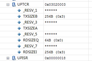
//config UPTCR---uPP Threshold Configuration Register (UPTCR)
upp_config.UPTCR.bits.RDSIZEI = 3;//Read threshold for DMA Channel I. Controls burst size for DMA Channel I.
//0h-64B,1h-128B,2h-reserved,3h-256B
upp_config.UPTCR.bits.TXSIZEB = 3; //设置通道B的发送大小门槛为256Byte add by wh 20140211
//0h-64B,1h-128B,2h-reserved,3h-256B
//config UPIES---uPP Interrupt Enabled Status Register (UPIER)
upp_config.UPIES.bits.EOLI= 0x01; //turn on EOL(end of line) interrupt for CHA(DMA channel I)
upp_config.UPIES.bits.EOWI= 0x01; //turn on EOW(end of window)interrupt for CHA(DMA channel I)
upp_config.UPIES.bits.EOLQ= 0x01; //turn on EOL(end of line) interrupt for CHB(DMA channel Q)add by wh 20140211
upp_config.UPIES.bits.EOWQ= 0x01; //turn on EOW(end of window)interrupt for CHB(DMA channel Q)add by wh 20140211
upp_config.UPPCR.bits.EN = 0x01; //Set the EN bit in the uPP peripheral control register (UPPCR) to 1 to turn on
the uPP peripheral.
//UPISR---uPP Interrupt Raw Status Register (UPISR) 中断状态寄存器
UPP_init(&upp_config);//初始化UPP口
}
===========================================
收发寄存器设置:
while(CHKBIT(UPP->UPIS2, 0x00000002)){};
UPP->UPID0 = (uint32_t)&upp_data_recv[0]; //接收缓冲区
UPP->UPID1 = 0x00040800; //4 lines per window 256*4 words per line
UPP->UPID2 = 0x00000800;
UPP->UPID2 = 0x00000800;
UPP->UPQD0 = (uint32_t)&upp_data_send; //发送缓冲区
UPP->UPQD1 = 0x00010800; //1 lines per window ,256*4 words per line
UPP->UPQD2 = 0x00000800;
UPP->UPQD2 = 0x00000800;
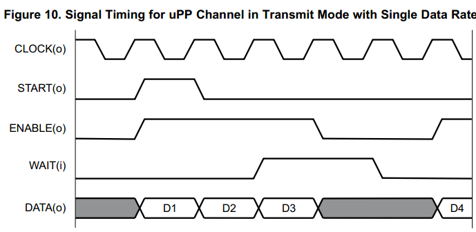
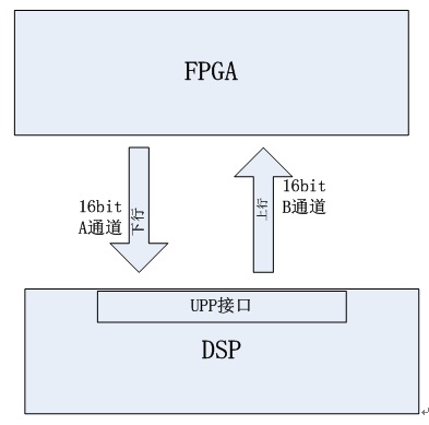
目前在调试TMS320VC6748 dsp,使用UPP口与FPGA接口,使用CHA从FPGA接收数据到DSP内计算,将计算结果通过UPP口的CHB通道发送 给FPGA;
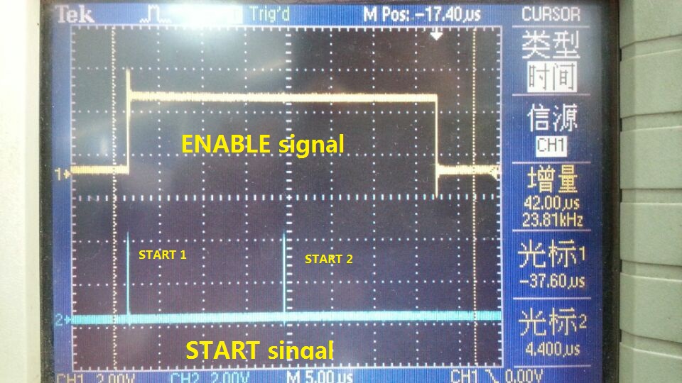
遇到的问题:CHB发送时,在FPGA侧每个ENABLE信号为高期间,会有2个START信号,明显不符合时序,这是什么原因?
我自己分析可能与如下设置有关:
upp_config.UPTCR.bits.TXSIZEB = 3; //设置通道B的发送大小门槛为256Byte add by wh 20140211
//0h-64B,1h-128B,2h-reserved,3h-256B
是不是每次发送256Byte就会有一个START脉冲?通过调整发送窗口的总量,及TXSIZEB的设置值,好像没有什么规律,请各位大神
帮忙分析一下啊。